|
|
|
PDF AUIRFS4127 Data sheet ( Hoja de datos )
| Número de pieza | AUIRFS4127 | |
| Descripción | Power MOSFET ( Transistor ) | |
| Fabricantes | Infineon | |
| Logotipo | ||
Hay una vista previa y un enlace de descarga de AUIRFS4127 (archivo pdf) en la parte inferior de esta página. Total 12 Páginas | ||
|
No Preview Available !
Features
Advanced Process Technology
Ultra Low On-Resistance
175°C Operating Temperature
Fast Switching
Repetitive Avalanche Allowed up to Tjmax
Lead-Free, RoHS Compliant
Automotive Qualified *
Description
Specifically designed for Automotive applications, this
HEXFET® Power MOSFET utilizes the latest processing
techniques to achieve extremely low on-resistance per silicon
area. Additional features of this design are a 175°C junction
operating temperature, fast switching speed and improved
repetitive avalanche rating . These features combine to make
this design an extremely efficient and reliable device for use in
Automotive applications and a wide variety of other applications.
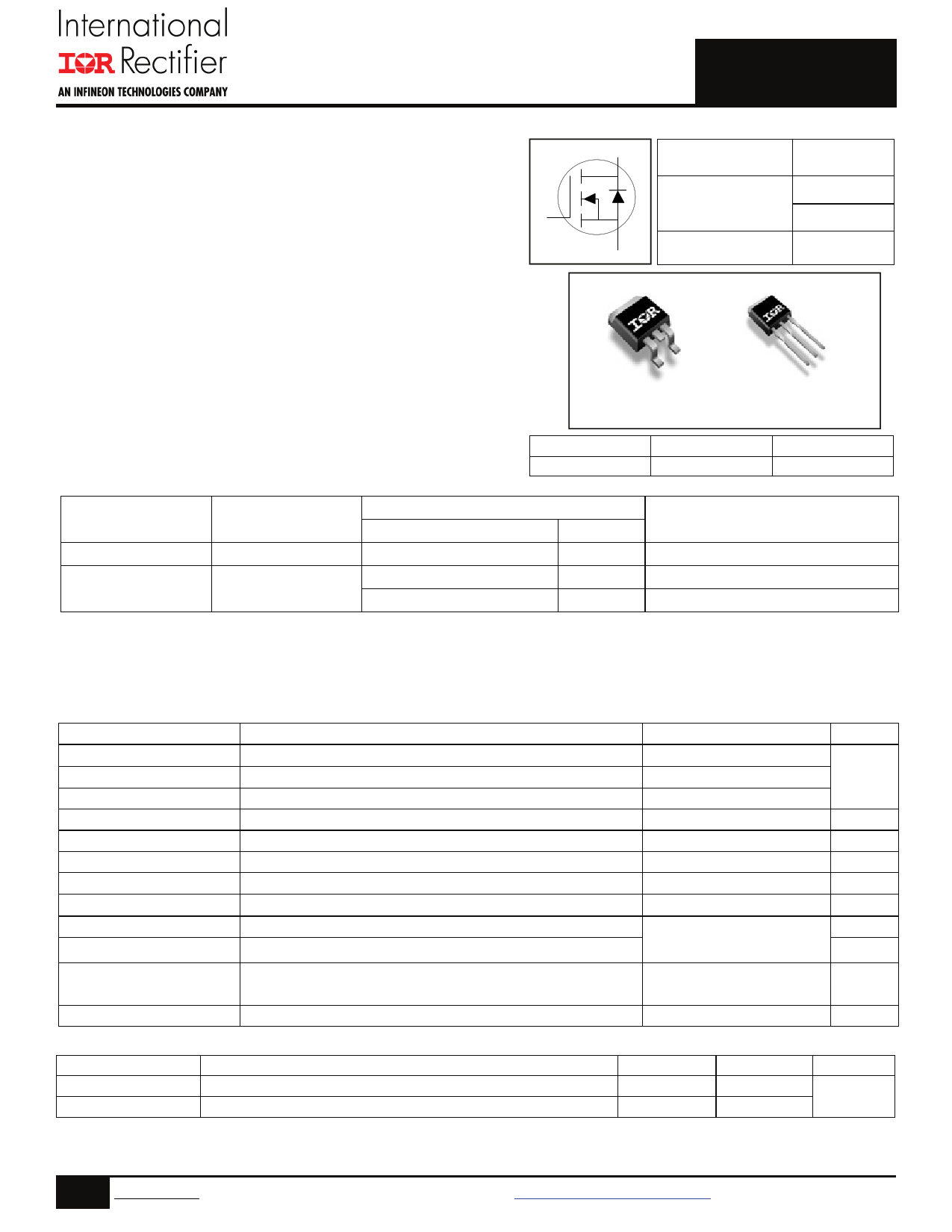
D
G
S
D
AUIRFS4127
AUIRFSL4127
HEXFET® Power MOSFET
VDSS
RDS(on) typ.
max
ID
200V
18.6m
22m
72A
D
S
G
D2Pak
AUIRFS4127
G
Gate
D
Drain
S
D
G
TO-262
AUIRFSL4127
S
Source
Base part number
AUIRFSL4127
AUIRFS4127
Package Type
TO-262
D2-Pak
Standard Pack
Form
Quantity
Tube
50
Tube
50
Tape and Reel Left
800
Orderable Part Number
AUIRFSL4127
AUIRFS4127
AUIRFS4127TRL
Absolute Maximum Ratings
Stresses beyond those listed under “Absolute Maximum Ratings” may cause permanent damage to the device. These are stress
ratings only; and functional operation of the device at these or any other condition beyond those indicated in the specifications is not
implied. Exposure to absolute-maximum-rated conditions for extended periods may affect device reliability. The thermal resistance
and power dissipation ratings are measured under board mounted and still air conditions. Ambient temperature (TA) is 25°C, unless
otherwise specified.
ID @ TC = 25°C
ID @ TC = 100°C
IDM
PD @TC = 25°C
VGS
dv/dt
EAS (Thermally limited)
IAR
EAR
TJ
TSTG
Parameter
Continuous Drain Current, VGS @ 10V
Continuous Drain Current, VGS @ 10V
Pulsed Drain Current
Power Dissipation
Linear Derating Factor
Gate-to-Source Voltage
Peak Diode Recovery
Single Pulse Avalanche Energy
Avalanche Current
Repetitive Avalanche Energy
Operating Junction and
Storage Temperature Range
Soldering Temperature for 10 seconds
Max.
72
51
300
375
2.5
± 20
57
250
See Fig. 14, 15, 22a, 22b
-55 to + 175
Units
A
W
W/°C
V
V/ns
mJ
A
mJ
°C
300(1.6mm from case)
Thermal Resistance
Symbol
Parameter
RJC
Junction-to-Case
RJA Junction-to-Ambient
Typ.
–––
–––
Max.
0.4
40
Units
°C/W
HEXFET® is a registered trademark of International Rectifier.
*Qualification standards can be found at http://www.irf.com/
1 www.irf.com © 2015 International Rectifier
Submit Datasheet Feedback
June 16, 2015
1 page 
1
AUIRFS/SL4127
D = 0.50
0.1 0.20
0.10
0.05
0.01 0.02
0.01
0.001
1E-006
SINGLE PULSE
( THERMAL RESPONSE )
1E-005
0.0001
0.001
t1 , Rectangular Pulse Duration (sec)
Notes:
1. Duty Factor D = t1/t2
2. Peak Tj = P dm x Zthjc + Tc
0.01 0.1
Fig 13. Maximum Effective Transient Thermal Impedance, Junction-to-Case
100
Duty Cycle = Single Pulse
0.01
Allowed avalanche Current vs avalanche
pulsewidth, tav, assuming Tj = 150°C and
Tstart =25°C (Single Pulse)
10
0.05
0.10
1 Allowed avalanche Current vs avalanche
pulsewidth, tav, assuming j = 25°C and
Tstart = 150°C.
0.1
1.0E-06
1.0E-05
1.0E-04
tav (sec)
1.0E-03
1.0E-02
1.0E-01
Fig 14. Avalanche Current vs. Pulse Width
250
TOP Single Pulse
BOTTOM 1% Duty Cycle
200 ID = 44A
150
100
50
0
25
50 75 100 125 150
Starting TJ , Junction Temperature (°C)
175
Fig 15. Maximum Avalanche Energy vs. Temperature
Notes on Repetitive Avalanche Curves , Figures 14, 15:
(For further info, see AN-1005 at www.irf.com)
1.Avalanche failures assumption:
Purely a thermal phenomenon and failure occurs at a
temperature far in excess of Tjmax. This is validated for every
part type.
2. Safe operation in Avalanche is allowed as long asTjmax is not
exceeded.
3. Equation below based on circuit and waveforms shown in Figures
22a, 22b.
4. PD (ave) = Average power dissipation per single avalanche pulse.
5. BV = Rated breakdown voltage (1.3 factor accounts for voltage
increase during avalanche).
6. Iav = Allowable avalanche current.
7. T = Allowable rise in junction temperature, not to exceed Tjmax
(assumed as 25°C in Figure 14, 15).
tav = Average time in avalanche.
D = Duty cycle in avalanche = tav ·f
ZthJC(D, tav) = Transient thermal resistance, see Figures 14)
PD (ave) = 1/2 ( 1.3·BV·Iav) = T/ ZthJC
Iav = 2T/ [1.3·BV·Zth]
EAS (AR) = PD (ave)·tav
5 www.irf.com © 2015 International Rectifier
Submit Datasheet Feedback
June 16, 2015
5 Page 
AUIRFS/SL4127
Qualification Information†
Qualification Level
Automotive
(per AEC-Q101)††
Comments: This part number(s) passed Automotive qualification. IR’s
Industrial and Consumer qualification level is granted by extension of the
higher Automotive level.
Moisture Sensitivity Level
ESD
Human Body Model
Charged Device Model
3L-D2 PAK
3L– TO-262
MSL1
N/A
Class H2 (+/- 4000V)††
AEC-Q101-001
Class C5 (+/- 2000V)††
AEC-Q101-005
RoHS Compliant
Yes
† Qualification standards can be found at International Rectifier’s web site: http//www.irf.com/
†† Highest passing voltage.
11 www.irf.com © 2015 International Rectifier
Submit Datasheet Feedback
June 16, 2015
11 Page | ||
| Páginas | Total 12 Páginas | |
| PDF Descargar | [ Datasheet AUIRFS4127.PDF ] | |
Hoja de datos destacado
| Número de pieza | Descripción | Fabricantes |
| AUIRFS4127 | Power MOSFET ( Transistor ) | Infineon |
| AUIRFS4127 | Power MOSFET ( Transistor ) | Infineon |
| Número de pieza | Descripción | Fabricantes |
| SLA6805M | High Voltage 3 phase Motor Driver IC. |
Sanken |
| SDC1742 | 12- and 14-Bit Hybrid Synchro / Resolver-to-Digital Converters. |
Analog Devices |
|
DataSheet.es es una pagina web que funciona como un repositorio de manuales o hoja de datos de muchos de los productos más populares, |
| DataSheet.es | 2020 | Privacy Policy | Contacto | Buscar |