|
|
|
PDF VS-19TQ015SPbF Data sheet ( Hoja de datos )
| Número de pieza | VS-19TQ015SPbF | |
| Descripción | High Performance Schottky Rectifier | |
| Fabricantes | Vishay | |
| Logotipo | ||
Hay una vista previa y un enlace de descarga de VS-19TQ015SPbF (archivo pdf) en la parte inferior de esta página. Total 7 Páginas | ||
|
No Preview Available !
www.vishay.com
VS-19TQ015SPbF
Vishay Semiconductors
High Performance Schottky Rectifier, 19 A
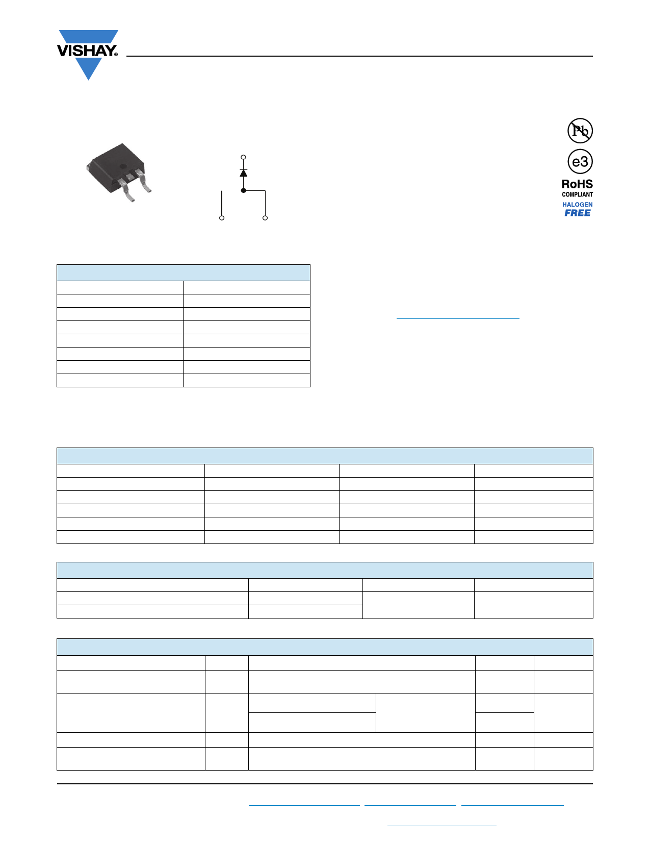
Base
cathode
2
D2PAK
1
N/C
3
Anode
PRODUCT SUMMARY
Package
IF(AV)
VR
VF at IF
IRM max.
TJ max.
Diode variation
EAS
D2PAK
19 A
15 V
0.36 V
522 mA at 100 °C
125 °C
Single die
6.75 mJ
FEATURES
• 125 °C TJ operation (VR < 5 V)
• Optimized for OR-ing applications
• Ultralow forward voltage drop
• High frequency operation
• Guard ring for enhanced ruggedness and long
term reliability
• High purity, high temperature epoxy
encapsulation for enhanced mechanical
strength and moisture resistance
• Meets MSL level 1, per J-STD-020, LF maximum peak
of 260 °C
• AEC-Q101 qualified
• Material categorization: for definitions of compliance
please see www.vishay.com/doc?99912
DESCRIPTION
The VS-19TQ015SPbF Schottky rectifier has been
optimized for ultralow forward voltage drop specifically for
the OR-ing of parallel power supplies. The proprietary
barrier technology allows for reliable operation up to 125 °C
junction temperature. Typical applications are in parallel
switching power supplies, converters, reverse battery
protection, and redundant power subsystems.
MAJOR RATINGS AND CHARACTERISTICS
SYMBOL
CHARACTERISTICS
IF(AV)
VRRM
IFSM
VF
TJ
Rectangular waveform
tp = 5 μs sine
19 Apk, TJ = 75 °C
Range
VOLTAGE RATINGS
PARAMETER
Maximum DC reverse voltage
Maximum working peak reverse voltage
SYMBOL
VR
VRWM
VALUES
19
15
700
0.32
-55 to +125
VS-19TQ015SPbF
15
UNITS
A
V
A
V
°C
UNITS
V
ABSOLUTE MAXIMUM RATINGS
PARAMETER
Maximum average forward current
See fig. 5
SYMBOL
IF(AV)
TEST CONDITIONS
50 % duty cycle at TC = 80 °C, rectangular waveform
Maximum peak one cycle
non-repetitive surge current
See fig. 7
5 μs sine or 3 μs rect. pulse
Following any rated
IFSM load condition and with
10 ms sine or 6 ms rect. pulse rated VRRM applied
Non-repetitive avalanche energy
Repetitive avalanche current
EAS TJ = 25 °C, IAS = 1.50 A, L = 6 mH
IAR
Current decaying linearly to zero in 1 μs
Frequency limited by TJ maximum VA = 3 x VR typical
VALUES
19
700
330
6.75
1.50
UNITS
A
A
mJ
A
Revision: 28-May-14
1 Document Number: 94152
For technical questions within your region: [email protected], [email protected], [email protected]
THIS DOCUMENT IS SUBJECT TO CHANGE WITHOUT NOTICE. THE PRODUCTS DESCRIBED HEREIN AND THIS DOCUMENT
ARE SUBJECT TO SPECIFIC DISCLAIMERS, SET FORTH AT www.vishay.com/doc?91000
1 page 
D2PAK, TO-262
Outline Dimensions
Vishay High Power Products
DIMENSIONS FOR D2PAK in millimeters and inches
Conforms to JEDEC outline D2PAK (SMD-220)
(3) L1
(2)(3)
E
4
A
D
1 23
L2
BB
H
(2)
Detail A
2x e
2 x b2 C
2xb
0.010 M A M B
Lead assignments
Diodes
1. - Anode (two die)/open (one die)
2., 4. - Cathode
3. - Anode
Lead tip
A
c2
B
A
(E)
A
c
± 0.004 M B
Gauge
plane
0° to 8°
E1
View A - A
H
L3
L
A1
L4
Detail “A”
Rotated 90 °CW
Scale: 8:1
Pad layout
11.00
(0.43)
MIN.
(D1) (3)
17.90 (0.70)
15.00 (0.625)
2.32
(0.08)
MIN.
(3) 2.64 (0.103)
2.41 (0.096)
9.65
(0.38)
MIN.
3.81
(0.15)
MIN.
Plating
(4)
b1, b3
Base
Metal
B
Seating
plane
(c) c1 (4)
(b, b2)
Section B - B and C - C
Scale: None
SYMBOL
MILLIMETERS
MIN. MAX.
INCHES
MIN. MAX.
NOTES
A 4.06 4.83 0.160 0.190
A1 0.00 0.254 0.000 0.010
b 0.51 0.99 0.020 0.039
b1
0.51 0.89 0.020 0.035
4
b2 1.14 1.78 0.045 0.070
b3
1.14 1.73 0.045 0.068
4
c 0.38 0.74 0.015 0.029
c1
0.38 0.58 0.015 0.023
4
c2 1.14 1.65 0.045 0.065
D
8.51 9.65 0.335 0.380
2
Notes
(1) Dimensioning and tolerancing per ASME Y14.5 M-1994
(2) Dimension D and E do not include mold flash. Mold flash shall not
exceed 0.127 mm (0.005") per side. These dimensions are
measured at the outmost extremes of the plastic body
(3) Thermal pad contour optional within dimension E, L1, D1 and E1
(4) Dimension b1 and c1 apply to base metal only
(5) Datum A and B to be determined at datum plane H
(6) Controlling dimension: inch
SYMBOL
D1
E
E1
e
H
L
L1
L2
L3
L4
MILLIMETERS
MIN. MAX.
6.86 8.00
9.65 10.67
7.90 8.80
2.54 BSC
14.61 15.88
1.78 2.79
- 1.65
1.27 1.78
0.25 BSC
4.78 5.28
INCHES
MIN. MAX.
0.270 0.315
0.380 0.420
0.311 0.346
0.100 BSC
0.575 0.625
0.070 0.110
- 0.066
0.050 0.070
0.010 BSC
0.188 0.208
NOTES
3
2, 3
3
3
(7) Outline conforms to JEDEC outline TO-263AB
Document Number: 95014
Revision: 31-Mar-09
For technical questions concerning discrete products, contact: [email protected]
For technical questions concerning module products, contact: [email protected]
www.vishay.com
1
5 Page | ||
| Páginas | Total 7 Páginas | |
| PDF Descargar | [ Datasheet VS-19TQ015SPbF.PDF ] | |
Hoja de datos destacado
| Número de pieza | Descripción | Fabricantes |
| VS-19TQ015SPbF | High Performance Schottky Rectifier | Vishay |
| Número de pieza | Descripción | Fabricantes |
| SLA6805M | High Voltage 3 phase Motor Driver IC. |
Sanken |
| SDC1742 | 12- and 14-Bit Hybrid Synchro / Resolver-to-Digital Converters. |
Analog Devices |
|
DataSheet.es es una pagina web que funciona como un repositorio de manuales o hoja de datos de muchos de los productos más populares, |
| DataSheet.es | 2020 | Privacy Policy | Contacto | Buscar |