|
|
|
PDF GS1675 Data sheet ( Hoja de datos )
| Número de pieza | GS1675 | |
| Descripción | SD/HD SDI Reclocker | |
| Fabricantes | GENNUM | |
| Logotipo | ||
Hay una vista previa y un enlace de descarga de GS1675 (archivo pdf) en la parte inferior de esta página. Total 30 Páginas | ||
|
No Preview Available !
GS1675 SD/HD SDI Reclocker
The GS1675 is a multi-rate serial digital reclocker designed to automatically recover the embedded clock from a digital video signal and
retime the incoming video data. It will recover the embedded clock signal and retime the data from a SMPTE 292M or SMPTE 259M-C
compliant digital video signal.
The GS1675 can operate in either Auto or Manual rate selection mode. In Auto mode, the device will automatically detect and lock onto
incoming SMPTE SDI data signals at SD and HD data rates. For single-rate data systems, the GS1675 can be configured to operate in
Manual mode. In both modes, the device requires only one external crystal to set the VCO frequency when not locked, and provides
adjustment-free operation. In systems which require passing non-SMPTE data rates, the GS1675 can be configured to either
automatically or manually enter a bypass mode in order to pass the signal without reclocking.
The GS1675 accepts industry-standard differential input levels including LVPECL and CML. The differential data and clock outputs
feature selectable output swing via the host interface, ensuring compatibility with most industry-standard, terminated differential
receivers. The GS1675 features dual differential outputs. The second output can be configured to emit either the recovered clock signal
or the re-timed video data.
Key Features
• SMPTE 292M and SMPTE 259M-C compliant
• Supports DVB-ASI at 270Mb/s
• Single-supply operation at 3.3V or 2.5V
• 180mW typical power consumption (213mW with RCO
enabled) at 2.5V
• 2:1 input multiplexer patented technology
• Choice of dual reclocked data outputs or one reclocked data
output and one clock output
• Uses standard 27MHz crystal
• Differential inputs and outputs
supports DC-coupling to industry-standard differential
logic
on-chip 100Ω differential data input/output termination
selectable 400mVppd or 800mVppd output swing on
each output
• 4-wire SPI host interface for device configuration and
monitoring
• Standard logic control and status signal levels
• Auto and Manual modes for rate selection
• Standards indication in Auto mode
• Lock Detect Output
• Mute, Bypass and Autobypass functions
• SD/HD indication output to control GS1678 or GS1679 cable
drivers
• Operating temperature range: -40°C to +85°C
• 32 pin 5mm x 5mm QFN package
• Pb-free and RoHS compliant
• Forward pin-compatible with the Gennum's 3G GS2965
reclocker
•
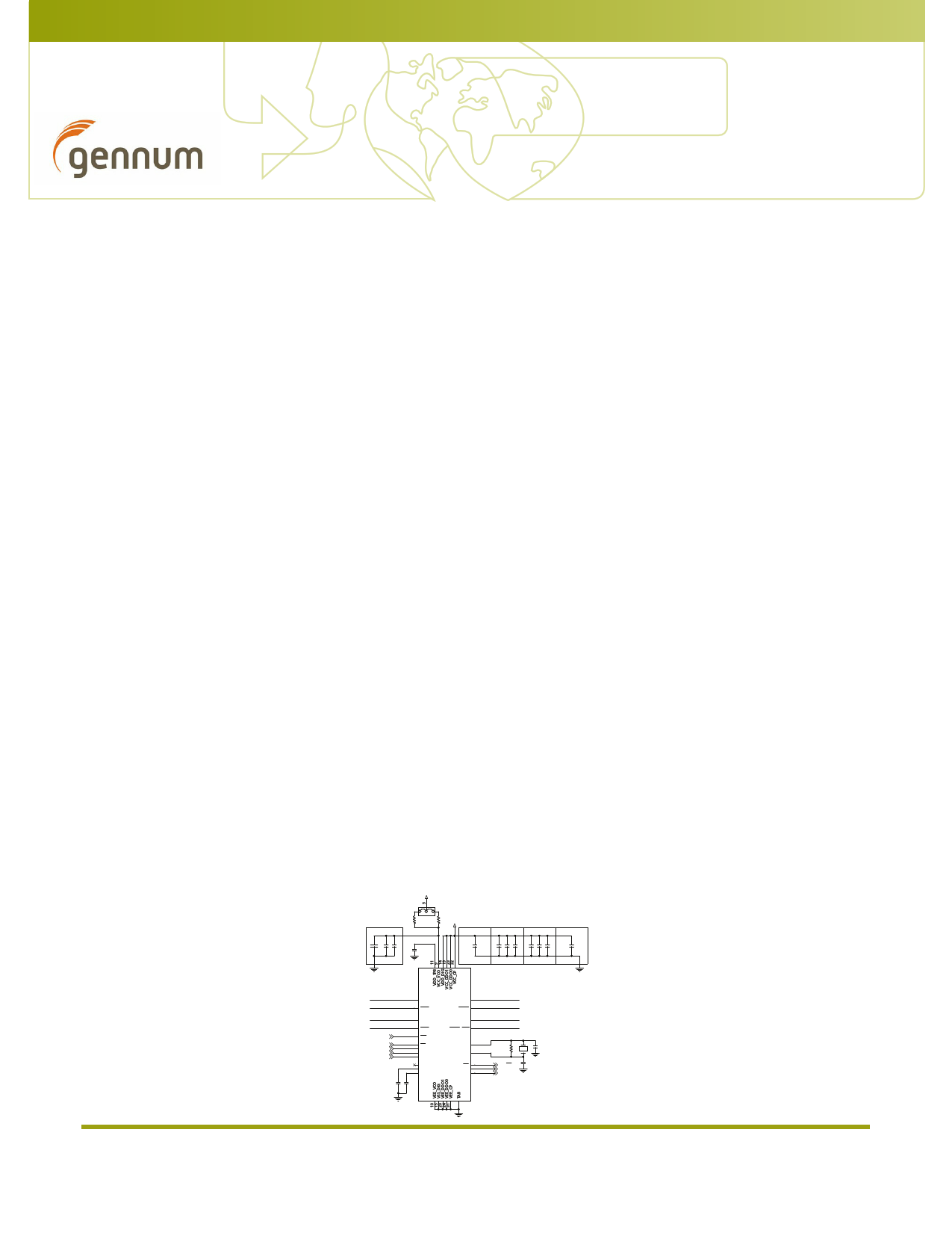
Typical Application Circuit
GS1675 SD/HD SDI Reclocker
Data Sheet
54174 - 1
June 2011
VCC2
JP5
VCO_SEL
2
R23
VCC_VCO
(Pin9)
422R
1
R24
VCC2
267R
C33 C31 C30
10u 1u 10n
VEE_VCO
(Pin10)
C34
220n
GND
U2
GND
VDD_DIG
(Pin14)
C32
10n
VSS_DIG
(Pin15)
VCC_DDO1
(Pin19)
VCC_DDO0
(Pin23)
C20 C23 C27 C13 C15 C16
10n DNPDNP 10n DNPDNP
VEE_DDO1
(Pin20)
VEE_DDO0
(Pin24)
VCC_CP
(Pin32)
C7
10n
VEE_CP
(Pin31)
GND
Data Input 0
Data Input 1
HIFb
CSb
SPI
SCK
SDO
SDI
C3
47n
3 DDI0
5
DDI0
DDO0 22
DDO0 21
6
7
4
27
28
29
30
8
1
2
C4
220n
DDI1
DDI1
HIF
CS
SCK
SDO
SDI
NC
LF+
CP_CAP
DDO1/RCO
DDO1/RCO
GS1675
XTAL-
XTAL+
SD/HD
LOS
LOCKED
18
17
26
25
16
13
12
GND
GND
Data Output 0
Data Output 1
ABM7-27.000MHZ-D2Y-T
R6 Y1
C1
18p
1M GND
C2
SD/HD
LOS
LOCKED
18p
GND
www.gennum.com
1 of 37
1 page 
1.2 Pin Descriptions
Table 1-1: GS1675 Pin Descriptions
Pin Number
1
Name
LF+
Type
Passive
2
CP_CAP
Power
3, 5
DDI0, DDI0
Input
4 HIF Logic Input
6, 7
DDI1, DDI1
Input
8
RSVD
Reserved
9
VCC_VCO
Power
10
11
12
13
14
15
16
17, 18
19
20
21, 22
23
24
VEE_VCO
VDD_1P8
LOCKED
LOS
VDD_DIG
VSS_DIG
SD/HD
DDO1/RCO,
DDO1/RCO
VCC_DDO1
VEE_DDO1
DDO0, DDO0
VCC_DDO0
VEE_DDO0
Power
Power
Output
Output
Power
Power
Output
Output
Power
Power
Output
Power
Power
25
XTAL+
Output
Description
Loop Filter Capacitor connection (CLF = 47nF). Connect as shown in the
Typical Application Circuit on page 30.
External capacitor for internal LDO regulator supplying the charge pump
circuit.
Serial Digital Differential Input 0.
Host interface selection pin. Active-low input. See Section 3.14.1.
Serial Digital Differential Input 1.
Reserved pin. Do not connect to this pin.
Most positive power supply connection for the internal
VCO section. Connect to a 3.3V supply with a 422Ω resistor, or a 2.5V
supply with a 267Ω resistor.
Most negative power supply connection for the internal
VCO section. Connect to GND.
External capacitor for internal 1.8V digital supply.
Lock Detect status signal. HIGH when the PLL is locked.
Loss Of Signal status. HIGH when the input signal is invalid.
Most positive power supply connection for the digital core.
Connect to 3.3V or 2.5V.
Most negative power supply for the digital core.
Connect to GND.
This signal will be LOW for all rates other than 270Mb/s.
This signal is HIGH for 270Mb/s.
Differential serial clock or data outputs.
Most positive power supply connection for the DDO1/DDO1 output driver.
Connect to 3.3V or 2.5V.
Most negative power supply connection for the DDO1/DDO1 output
driver. Connect to GND.
Differential Serial Digital Outputs.
Most positive power supply connection for the DDO0/DDO0 output driver.
Connect to 3.3V or 2.5V.
Most negative power supply connection for the DDO0/DDO0 output
driver.
Connect to GND.
Reference crystal output.
GS1675 SD/HD SDI Reclocker
Data Sheet
54174 - 1
June 2011
5 of 37
5 Page 
3. Functional Description
The GS1675 is a multi-standard reclocker for serial digital SDTV signals operating at
270Mb/s, and HDTV signals operating at 1.485Gb/s, 1.485/1.001Gb/s.
3.1 Serial Data Input
The GS1675 features two differential input buffers.
The serial data input signal is connected to the DDI0/DDI0 and DDI1/DDI1 input pins of
the device.
Input signals can be single-ended or differential, DC or AC-coupled.
The input circuit is self-biasing, to allow for simple AC or DC-coupling of input signals to
the device.
The serial digital data inputs are also compatible when DC-coupled with LVPECL or
CML differential outputs from crosspoint switches which operate from 3.3V or 2.5V
supplies. This includes but is not limited to the GS1674 Equalizer.
3.2 Modes of Operation
The GS1675 has two modes of operation: Legacy Mode (HIF = HIGH) and SPI Mode (HIF
= LOW).
In Legacy Mode, chip functions are controlled via pins only, and offers limited control of
input equalization.
In SPI mode, access is gained to extended digital controls like: Bypass, Autobypass,
Auto/Manual selection, Control status inputs or outputs, changes to KBB settings, as well
as access to additional features such as LOS adjustment, polarity invert, auto-mute, etc.
3.3 2:1 Input Mux
The GS1675 incorporates a 2:1 input mux, which allows the connection of two
independent streams of video/data. There are two differential inputs (DDI[1:0] /
DDI[1:0]). The active channel can be selected via the DDI_SEL[1:0] registers as shown in
Table 3-1.
Table 3-1: Input Selection Table
DDI_SEL[1:0]
00
01
10
11
* Power-up default
Selected Input
DDI0*
NOT VALID
NOT VALID
DDI1
GS1675 SD/HD SDI Reclocker
Data Sheet
54174 - 1
June 2011
11 of 37
11 Page | ||
| Páginas | Total 30 Páginas | |
| PDF Descargar | [ Datasheet GS1675.PDF ] | |
Hoja de datos destacado
| Número de pieza | Descripción | Fabricantes |
| GS1670 | HD/SD SDI Receiver Complete | Semtech |
| GS1670A | HD/SD SDI Receiver | Semtech |
| GS1671A | HD/SD SDI Receiver | Semtech |
| GS1672 | HD/SD-SDI Serializer | GENNUM |
| Número de pieza | Descripción | Fabricantes |
| SLA6805M | High Voltage 3 phase Motor Driver IC. |
Sanken |
| SDC1742 | 12- and 14-Bit Hybrid Synchro / Resolver-to-Digital Converters. |
Analog Devices |
|
DataSheet.es es una pagina web que funciona como un repositorio de manuales o hoja de datos de muchos de los productos más populares, |
| DataSheet.es | 2020 | Privacy Policy | Contacto | Buscar |