|
|
PDF LC72717PW Data sheet ( Hoja de datos )
| Número de pieza | LC72717PW | |
| Descripción | Mobile FM Multiplex Broadcast (DARC) Receiver IC | |
| Fabricantes | ON Semiconductor | |
| Logotipo | ||
Hay una vista previa y un enlace de descarga de LC72717PW (archivo pdf) en la parte inferior de esta página. Total 27 Páginas | ||
|
No Preview Available !
Ordering number : ENA2064D
LC72717PW
CMOS IC
Mobile FM Multiplex Broadcast
(DARC) Receiver IC
http://onsemi.com
Overview
The LC72717PW is a data demodulation LSI for receiving FM multiplex broadcasts for mobile reception in the
DARC format. This LSI includes an on-chip bandpass filter for extracting the DARC signal from the FM baseband
signal. It also supports ITU-R recommended FM multiplex frame structures (methods A, A’, B, and C) and can
implement a compact, multifunction DARC reception system.
The LC72717PW’s package, pin assignment and electrical characteristics are same as the LC72715PW (VICS-LSI).
Functionally, the LC72717PW is a product that VICS function is removed from the LC72715PW.
The LC72717PW is also control-compatible with the LC72711LW.
Note that a contract with the NHK Engineering System, Inc. may be required to produce DARC compatible
products in case, please contact with the NHK Engineering System, Inc.
Functions
Adjustment-free 76kHz SCF bandpass filter
Supports all FM multiplex frame structures
(methods A, A’, B and C) under CPU control.
MSK delay detection system based on a 1T delay.
Error correction function based on a 2T delay
(in the MSK detection stage)
Digital PLL based clock regeneration function
Shift-register 1T and 2T delay circuits
Block and frame synchronization detection circuits
Functions for setting the number of allowable BIC errors
and the number of synchronization protection operations.
Error correction using (272, 190) codes
SQFP64(10X10)
Built-in layer 4 CRC code checking circuit
On-chip frame memory and memory control circuit for vertical correction
7.2MHz crystal oscillator circuit
Two power saving modes: STNBY and EC STOP
Applications can use either a parallel CPU interface (DMA) or a CCB serial interface.
Supply voltage: 2.7V to 3.6V
CCB is ON Semiconductor® ’s original format. All addresses are managed
by ON Semiconductor® for this format.
CCB is a registered trademark of Semiconductor Components Industries, LLC.
ORDERING INFORMATION
See detailed ordering and shipping information on page 27 of this data sheet.
Semiconductor Components Industries, LLC, 2014
March, 2014
30314HK 20140226-S00002/O3013HK 20131021-S00002
/32713HKPC/80812HK/53012HK No.A2064-1/27
1 page 
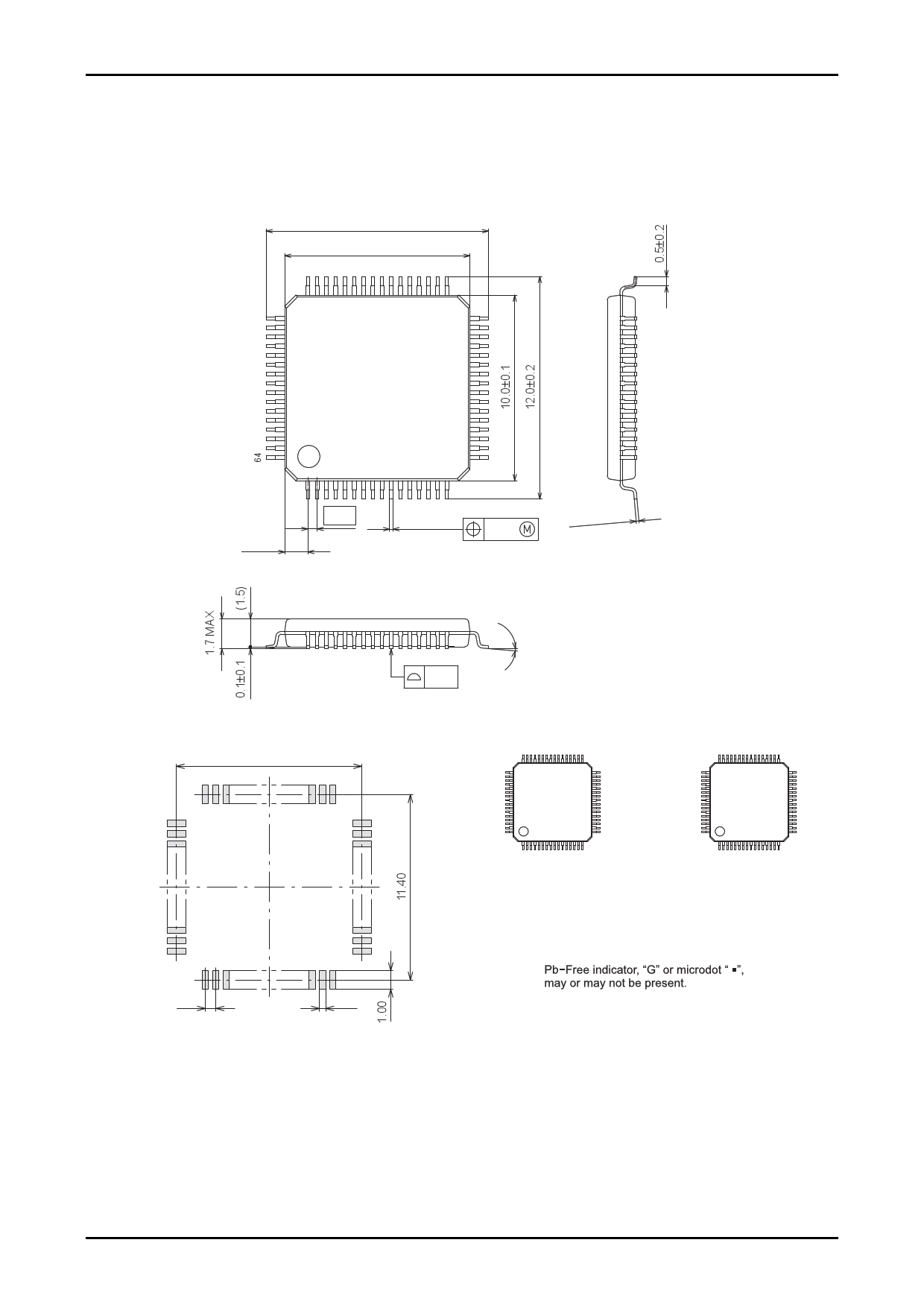
Package Dimensions
unit : mm
SPQFP64 10x10 / SQFP64
CASE 131AK
ISSUE A
LC72717PW
12.0±0.2
10.0±0.1
(1.25)
1 2 0.5
0.18
+0.08
−0.03
0.10
0.15±0.05
0 to10°
0.10
SOLDERING FOOTPRINT*
11.40
(Unit: mm)
GENERIC MARKING DIAGRAM*
XXXXXXXX
YDD
XXXXXXXX
YMDDD
XXXXX = Specific Device Code
Y = Year
DD = Additional Traceability Data
XXXXX = Specific Device Code
Y = Year
M = Month
DDD = Additional Traceability Data
*This information is generic. Please refer to
device data sheet for actual part marking.
0.50 0.28
NOTE: The measurements are not to guarantee but for reference only.
*For additional information on our Pb−Free strategy and soldering
details, please download the ON Semiconductor Soldering and
Mounting Techniques Reference Manual, SOLDERRM/D.
No.A2064-5/27
5 Page 
LC72717PW
Symbol
tCL
tCH
tSU
tHD
tEL
tES
tEH
tLC
tDDO*1
TDDO2
tCRC
Parameter
Clock “L” level time
Clock “H” level time
Data setup time
Data hold time
CE wait time
CE setup time
CE hold time
Data latch change time
DO data output time
DO data output off time
CRC4 change period
min
0.7
0.7
0.7
0.7
0.7
0.7
0.7
typ
135
135
max
0.7
320
0.7
unit
s
s
s
s
s
s
s
s
ns
ns
s
*1 DO data output change time from the “H” level to the “L” level. Output change time from the “L” level to the “H”
level is determined by the external pull-up resistance value and load capacitance value.
CPU Interface <Parallel Mode>
This LSI can perform control via the parallel interface, in addition to the CCB interface. To use the parallel interface, it
is necessary to set the SP pin = L. The data bus width can be selected with the BUSWD pin. (BUSWD pin - L: 8 bits,
H: 16 bits)
The DMA transmission method can also be selected according to the setting of control register.
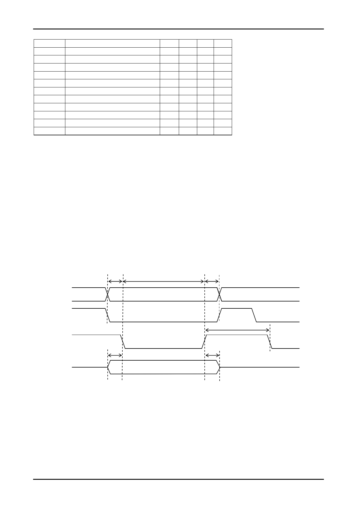
(1) Data input (register setting)
Data is set to the register in LSI. For accessing, input the register address to A0 to A3 pins and the write data to the
D(n) pin.
Set the CS pin = L, and then the WR pin = L. Subsequently, by setting the WR pin = H and the CS pin = H after the
tWWRL period, the data can be set to the register. It is necessary to keep an interval of tCYWR or more before the
next data input.
A0 to A3
tSAWR
tWWRL
tHAWR
CS
WR
D(n)
tWDS
tCYWR
tWDH
No.A2064-11/27
11 Page | ||
| Páginas | Total 27 Páginas | |
| PDF Descargar | [ Datasheet LC72717PW.PDF ] | |
Hoja de datos destacado
| Número de pieza | Descripción | Fabricantes |
| LC72717PW | Mobile FM Multiplex Broadcast (DARC) Receiver IC | ON Semiconductor |
| Número de pieza | Descripción | Fabricantes |
| SLA6805M | High Voltage 3 phase Motor Driver IC. |
Sanken |
| SDC1742 | 12- and 14-Bit Hybrid Synchro / Resolver-to-Digital Converters. |
Analog Devices |
|
DataSheet.es es una pagina web que funciona como un repositorio de manuales o hoja de datos de muchos de los productos más populares, |
| DataSheet.es | 2020 | Privacy Policy | Contacto | Buscar |
