|
|
|
PDF VT1115M Data sheet ( Hoja de datos )
| Número de pieza | VT1115M | |
| Descripción | MULTIPHASE SWITCHING REGULATOR | |
| Fabricantes | Volterra Semiconductor | |
| Logotipo | ||
Hay una vista previa y un enlace de descarga de VT1115M (archivo pdf) en la parte inferior de esta página. Total 30 Páginas | ||
|
No Preview Available !
PRELIMINARY
VT1115M CHIPSET
REVISION - December 30, 2004
PROGRAMMABLE OUTPUT, MULTIPHASE SWITCHING
REGULATOR WITH SMBus
Smart
Slave™
VT1105S
VT1125S
Input
Voltage
7V to
13.2V
Output
Voltage
0.600V to
1.600V
Current
Rating
25A per
Phase
VID
VRs
10.X, 11 &
Opteron™
GENERAL DESCRIPTION
Volterra’s fourth-generation chipset is a complete, integrated,
scalable architecture for the highest density multiphase
synchronous buck regulators. This ultra high density solu-
tion minimizes external components and offers enhanced
regulator performance, comprehensive control and reporting
features, ease of design and the smallest footprint available
for demanding multiphase synchronous buck converters. The
chipset is targeted for applications such as servers and net-
working systems.
The VT1115M master is part of the Volterra Generation 4
architecture as shown in Figure 1. Each VT1115M drives
and controls multiple Generation 4 Smart Slave™ integrated
output devices, such as the VT1105S and VT1125S. The
number of Generation 4 Smart Slaves™ can be set by design,
according to the application requirements. The desired slave
and load operating conditions are controlled by a desired
current command issued from the VT1115M to the slave
devices. Configuration and monitoring of the VR conditions
are controlled via an interconnecting bus between the master
and the slaves as shown in Figure 1.
The VT1115M supports the following voltage regulator speci-
fications: Intel® VR 10 and extended VR 10, AMD Opteron™
and Intel® VR 11.
The architecture incorporates a SMBus interface for monitor-
ing and control of the voltage regulator. Regulator parameters
can be set and monitored via the two-way SMBus for control,
protection and shutdown of the regulator. The SMBus can
provide a reading of faults such as VX short-circuit or slave
over-temperature, so that the regulator can be controlled and
protected during all operating conditions. The SMBus can
also provide temperature readings of individual slaves.
A key benefit of the architecture is that it provides excellent
scalability by increasing the number of slaves per system.
This flexibility allows the designer to trade-off cost and perfor-
mance for a given application using one VT1115M controller
and different slave configurations with no redesign or re-layout.
The number of phases and output current requirement can
be determined by the designer and easily populated or de-
populated to meet different load and performance targets.
KEY FEATURES
• Smallest Footprint: Typical Solution Occupies Less
than 1600mm2 in a 150A VRM Application
• Lowest Profile: 5mm Maximum Height
• Highest Accuracy Current Sharing
• Up to 25A/Phase Output – Programmable
• Differential Voltage Sense at Point of Load
• Scalable Output Current: Up to 8 Slaves
• SMBus Interface
• Output Status Reporting and Shutdown
• Slave Temperature Reporting
• Factory Set Presets for High Performance Design
• Switching Frequency: 500kHz-1.5MHz
• 8-Bit VID Input, with 6.25mV Steps and Setpoint
Trim for Programmable VOUT
– Intel® VR 10.X: 0.83125V-1.60V
– Intel® Extended (7-Bit) VR 10.X
– Intel® VR 11: 0.6V-1.60V
– AMD Opteron™: 0.80V-1.55V
• Dynamic VID
• Programmable Setpoint and Droop
• Programmable VR_HOT and VR_FAN Functions
• Programmable OVP, OVLO and UVLO
• Cycle-by-Cycle Current Limiting
• Power Good, OVP, Fault Flags and Output Enable
• Redundant Inputs for Power Good and OVP
SYSTEMS
• Servers and Workstations
• Enterprise Storage
• Broadband Communication
• Networking
• Small Form Factor Desktops
APPLICATIONS
Voltage Regulator Modules (VRMs) and On-Board
Regulators (VR Down)
• Microprocessors (µP): 32 and 64 Bit I/A and RISC
Architectures
• Memory
• Graphics Processors
• Network, Chipset ICs
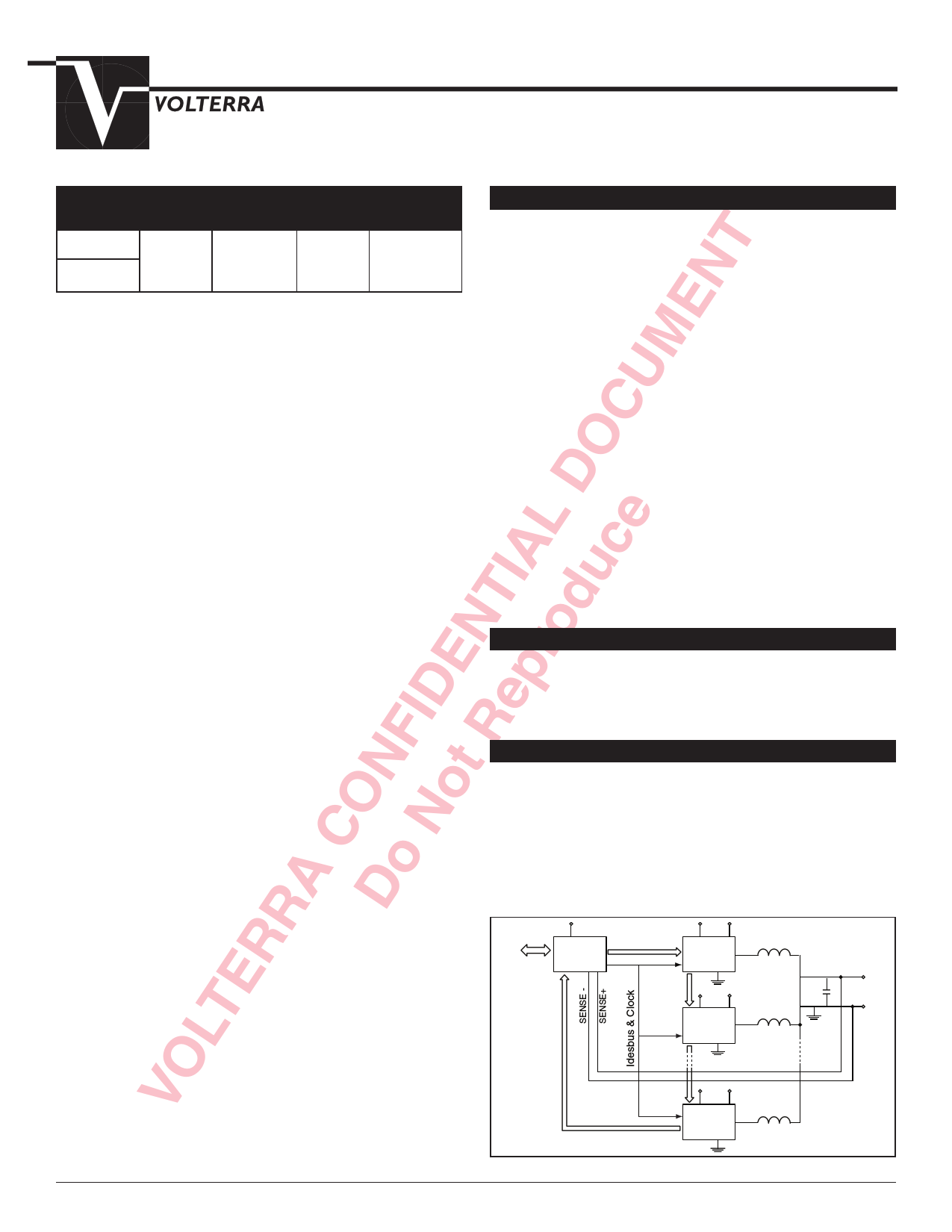
TYPICAL APPLICATION CIRCUIT
3.3V
SMBus
VT1115M
Master
Digital
Control Bus
3.3V 12V
VT11x5S VX1
Slave 1
LOUT1
3.3V 12V
VT11x5S VX2
Slave 2
LOUT2
COUT
VOUT
Output voltage, switching frequency, current per slave,
setpoint, droop, over- and undervoltage protection levels and
many other voltage regulator parameters are all programmed
easily on the VT1115M controller and communicated to the
slaves via a bus between master and slaves.
Volterra Semiconductor Corp. Proprietary. Do Not Copy. Do Not Distribute.
3.3V 12V
VT11x5S VXN
Slave N
LOUTN
Figure 1. VT1115M System Architecture
1
1 page 
PROPRIETARY AND CONFIDENTIAL
PRELIMINARY VT1115M CHIPSET
PROGRAMMABLE OUTPUT, MULTIPHASE SWITCHING REGULATOR WITH SMBus
ELECTRICAL CHARACTERISTICS (CONTINUED)
Symbol
Parameter
Conditions
Undervoltage and Overvoltage Lockout 12V Supply
IN_UVLORE
12V UVLO Reference Voltage
Rising Edge
IN_UVLOFE
12V UVLO Reference Voltage
Falling Edge
IN_OVLORE
12V OVLO Reference Voltage
Rising Edge
IN_OVLOFE
12V OVLO Reference Voltage
Falling Edge
tUVLO-RE,
12V UVLO and OVLO Rising- Includes time to shut
tOVLO-RE,
Edge Response Time
down the slave
tUVLO-FE,
12V UVLO and OVLO Falling- Not including soft-start
tOVLO-FE,
Edge Response Time
delay
Undervoltage Lockout 3.3V Supply (Master-Internal)
3_3V_UVLO
3.3V Internal UVLO
Rising threshold
Falling threshold
3_3V_UVLOHYSTERESIS Hysteresis
VR 11 Start-Up Timing (See Figure 18)
TD1
OE and UVLO to VCORE
After VCC/VDDH valid,
Starting to Ramp Delay
OE goes high and VR
configuration done
TD2
VCORE Slew Rate to
VBOOT = 1.1V
Minimum must be set
to comply with VR
specifications
TD3 Time to Wait to Read VID Code
TD4 Time to Regulate VID Code Minimum must be set
to comply with VR
specifications
TD5 Time Until VR Ready (Power
Good)
Second Level Redundancy (EXT_REF Pin)
VEXT_REF
EXT_REF Threshold
tEXT_REF
OVP
-
-
-
OCP
-
Fault Response Time
DC Threshold Error
Delay with VOUT 100mV Above
Threshold
OVP Lockout after DAC
Enabled (OE High, UVLO &
OVLO Low)
Threshold Error at IMAX
- Time-Out, PPM & CCM
- PPM Duty Cycle
Slave FAULTB Ball (VT1125S)
VOL-FAULTB
FAULTB Output Low Voltage With 4.7kΩ external pull-
up
RPULLDOWN-FAULTB
FAULTB Pull-Down Resistance
Min Typ Max Units
1.80 1.90 V
1.21 1.31 V
1.80 1.90 V
1.21 1.31 V
7.25 µs
7.25 µs
2.78 2.85
2.69 2.75
91 97 103
15
V
V
mV
ms
0.05 5 ms
50 3000 µs
0 250 2500 µs
50 3000 µs
-3 +3 %
VNOM
10 µs
-40 +40 mV
0.5 1.0
µs
1.6 2.0 2.4 ms
-10 +10 % of
IMAX
4 5 6 ms
10 %
0.1 0.4
50 200
V
Ω
REVISED - 12/30/04
Volterra Semiconductor Corp. Proprietary. Do Not Copy. Do Not Distribute. 5
5 Page 
PROPRIETARY AND CONFIDENTIAL
PRELIMINARY VT1115M CHIPSET
PROGRAMMABLE OUTPUT, MULTIPHASE SWITCHING REGULATOR WITH SMBus
DBI (Pin 26): Digital control bus input.
DBO (Pin 27): Digital control bus output.
R_SEL[7:0] (Pin 28, 31, 37, 38, 41-44): System configuration
resistors. (Programmable features detailed in Table 6.)
IDES_P (Pin 29): Idesired command (+).
IDES_N (Pin 30): Idesired command (-).
LOAD_CURRENT (Pin 32): Analog voltage representing
load current.
VIN_UV (Pin 33): Scaled version of slave VDDH voltage for
under voltage shutdown. This pin is used to program the input
undervoltage lockout threshold for the slave VDDH supply.
See the Undervoltage and Overvoltage Programming and
Protection section for additional design information.
VIN_OV (Pin 34): Scaled version of slave VDDH voltage
used for over voltage shutdown. This pin is used to program
the input overvoltage lockout threshold for the slave VDDH
supply. See the Undervoltage and Overvoltage Programming
and Protection section for additional design information.
R_FREQ (Pin 35): Resistor used to program switching
frequency.
R_REF (Pin 39): Reference resistor used to calibrate
R_SEL.
EXT_REF (Pin 45): Precision external reference input. High
reliability feature designed to guard against master controller
failures. If the VT1115M determines that the voltage on this
pin is out of range, it will shut down the system.
SD (Pin 46): Serial data pin for SMBus interface. See the
SMBus Communication with the VT1115M section for addi-
tional design information. When not in use, this pin should
be connected to VDD.
SC (Pin 47): Serial clock pin for SMBus interface. See the
SMBus Communication with the VT1115M section for addi-
tional design information. When not in use, this pin should
be connected to VDD.
PWRGD (Pin 48): Power good output pin. This pin indicates
whether the output voltage is within regulation. This open-
drain output should be externally pulled HIGH with a resistor.
See the Power Good and Undervoltage and Overvoltage
Programming and Protection sections for additional design
information.
REVISED - 12/30/04
Volterra Semiconductor Corp. Proprietary. Do Not Copy. Do Not Distribute. 11
11 Page | ||
| Páginas | Total 30 Páginas | |
| PDF Descargar | [ Datasheet VT1115M.PDF ] | |
Hoja de datos destacado
| Número de pieza | Descripción | Fabricantes |
| VT1115M | VOLTAGE CONTROLLED OSCILLATOR | CSGHK |
| VT1115M | MULTIPHASE SWITCHING REGULATOR | Volterra Semiconductor |
| Número de pieza | Descripción | Fabricantes |
| SLA6805M | High Voltage 3 phase Motor Driver IC. |
Sanken |
| SDC1742 | 12- and 14-Bit Hybrid Synchro / Resolver-to-Digital Converters. |
Analog Devices |
|
DataSheet.es es una pagina web que funciona como un repositorio de manuales o hoja de datos de muchos de los productos más populares, |
| DataSheet.es | 2020 | Privacy Policy | Contacto | Buscar |