|
|
|
PDF NUP4114UCLW1T2G Data sheet ( Hoja de datos )
| Número de pieza | NUP4114UCLW1T2G | |
| Descripción | TVS Diode ( Rectifier ) | |
| Fabricantes | ON Semiconductor | |
| Logotipo | ||
Hay una vista previa y un enlace de descarga de NUP4114UCLW1T2G (archivo pdf) en la parte inferior de esta página. Total 9 Páginas | ||
|
No Preview Available !
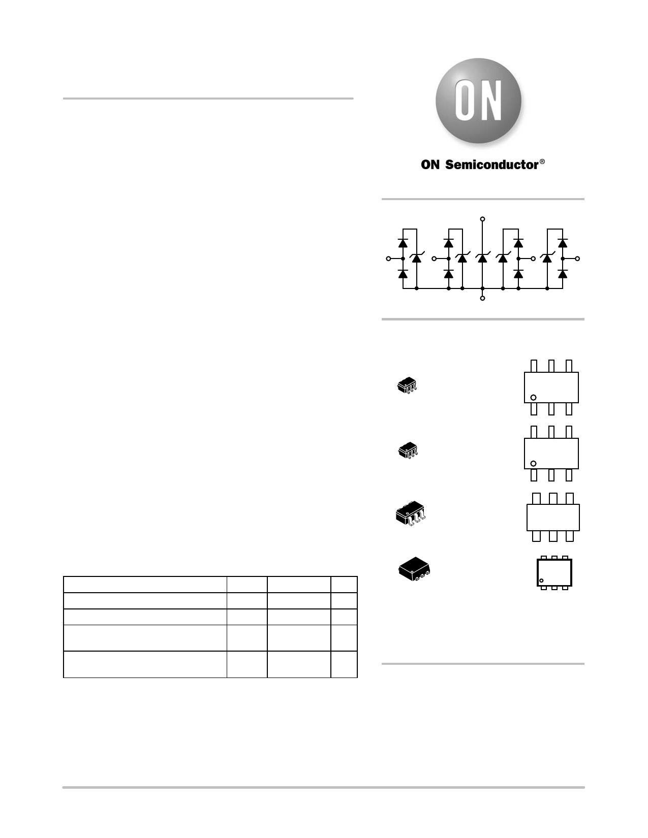
NUP4114 Series,
SZNUP4114 Series
Transient Voltage
Suppressors
ESD Protection Diodes with Low
Clamping Voltage
The NUP4114 transient voltage suppressors are designed to protect
high speed data lines from ESD. Ultra−low capacitance and high level
of ESD protection make these devices well suited for use in USB 2.0
high speed applications.
Features
• Low Clamping Voltage
• Small Body Outline Dimensions on SC−88 Package:
0.082″ x 0.078″ (2.10 mm x 1.25 mm)
• Low Body Height: 0.043″ (1.10 mm)
• Stand−off Voltage: 5.5 V
• Low Leakage
• Response Time is Typically < 1.0 ns
• IEC61000−4−2 Level 4 ESD Protection
• These Devices are Pb−Free and are RoHS Compliant
• AEC−Q101 Qualified and PPAP Capable − SZNUP4114
• SZ Prefix for Automotive and Other Applications Requiring Unique
Site and Control Change Requirements
Typical Applications
• LVDS
• USB 2.0 High Speed Data Line and Power Line Protection
• Digital Video Interface (DVI) and HDMI
• Monitors and Flat Panel Displays
• High Speed Communication Line Protection
• Notebook Computers
• Gigabit Ethernet
MAXIMUM RATINGS (TJ = 25°C unless otherwise noted)
Rating
Symbol
Value
Unit
Operating Junction Temperature Range TJ −40 to +125 °C
Storage Temperature Range
Tstg − 55 to +150 °C
Lead Solder Temperature −
Maximum (10 Seconds)
TL 260 °C
IEC 61000−4−2 (ESD)
Contact
Air
±8 kV
±15
Stresses exceeding those listed in the Maximum Ratings table may damage the
device. If any of these limits are exceeded, device functionality should not be
assumed, damage may occur and reliability may be affected.
http://onsemi.com
5
16
34
2
MARKING
DIAGRAMS
6
SC−88
W1 SUFFIX
1 CASE 419B
X2 MG
G
1
6
SC−88
W1 SUFFIX
1 CASE 419B
X4 MG
G
1
6
TSOP−6
CASE 318G
1 STYLE 12
P4H MG
G
1
6
1
SOT−563
CASE 463A
P4MG
G
1
XXX = Specific Device Code
M = Date Code
G = Pb−Free Package
(Note: Microdot may be in either location)
ORDERING INFORMATION
See detailed ordering and shipping information in the package
dimensions section on page 4 of this data sheet.
See Application Note AND8308/D for further description of survivability specs.
© Semiconductor Components Industries, LLC, 2014
September, 2014 − Rev. 3
1
Publication Order Number:
NUP4114/D
1 page 
NUP4114 Series, SZNUP4114 Series
APPLICATIONS INFORMATION
The new NUP4114 is a low capacitance TVS diode array
designed to protect sensitive electronics such as
communications systems, computers, and computer
peripherals against damage due to ESD events or transient
overvoltage conditions. Because of its low capacitance, it
can be used in high speed I/O data lines. The integrated
design of the NUP4114 offers low capacitance steering
diodes and a TVS diode integrated in a single package
(TSOP−6). If a transient condition occurs, the steering
diodes will drive the transient to the positive rail of the
power supply or to ground. The TVS device protects the
power line against overvoltage conditions to avoid damage
to the power supply and any downstream components.
NUP4114 Configuration Options
The NUP4114 is able to protect up to four data lines
against transient overvoltage conditions by driving them to
a fixed reference point for clamping purposes. The steering
diodes will be forward biased whenever the voltage on the
protected line exceeds the reference voltage (Vf or
VCC + Vf). The diodes will force the transient current to
bypass the sensitive circuit.
Data lines are connected at pins 1, 3, 4 and 6. The negative
reference is connected at pin 2. This pin must be connected
directly to ground by using a ground plane to minimize the
PCB’s ground inductance. It is very important to reduce the
PCB trace lengths as much as possible to minimize parasitic
inductances.
Option 1
Protection of four data lines and the power supply using
VCC as reference.
Option 2
Protection of four data lines with bias and power supply
isolation resistor.
I/O 1
I/O 2
1
2
VCC
6
10 k
5
34
I/O 3
I/O 4
The NUP4114 can be isolated from the power supply by
connecting a series resistor between pin 5 and VCC. A 10 kW
resistor is recommended for this application. This will
maintain a bias on the internal TVS and steering diodes,
reducing their capacitance.
Option 3
Protection of four data lines using the internal TVS diode
as reference.
I/O 1
I/O 2
16
2 5 NC
I/O 1
I/O 2
1
6
I/O 3
I/O 4
3
4
I/O 3
I/O 4
2
3
5 VCC
4
For this configuration, connect pin 5 directly to the
positive supply rail (VCC), the data lines are referenced to
the supply voltage. The internal TVS diode prevents
overvoltage on the supply rail. Biasing of the steering diodes
reduces their capacitance.
In applications lacking a positive supply reference or
those cases in which a fully isolated power supply is
required, the internal TVS can be used as the reference. For
these applications, pin 5 is not connected. In this
configuration, the steering diodes will conduct whenever the
voltage on the protected line exceeds the working voltage of
the TVS plus one diode drop (VC = Vf + VTVS).
ESD Protection of Power Supply Lines
When using diodes for data line protection, referencing to
a supply rail provides advantages. Biasing the diodes
reduces their capacitance and minimizes signal distortion.
http://onsemi.com
5
5 Page | ||
| Páginas | Total 9 Páginas | |
| PDF Descargar | [ Datasheet NUP4114UCLW1T2G.PDF ] | |
Hoja de datos destacado
| Número de pieza | Descripción | Fabricantes |
| NUP4114UCLW1T2G | TVS Diode ( Rectifier ) | ON Semiconductor |
| Número de pieza | Descripción | Fabricantes |
| SLA6805M | High Voltage 3 phase Motor Driver IC. |
Sanken |
| SDC1742 | 12- and 14-Bit Hybrid Synchro / Resolver-to-Digital Converters. |
Analog Devices |
|
DataSheet.es es una pagina web que funciona como un repositorio de manuales o hoja de datos de muchos de los productos más populares, |
| DataSheet.es | 2020 | Privacy Policy | Contacto | Buscar |