|
|
|
PDF GA1087 Data sheet ( Hoja de datos )
| Número de pieza | GA1087 | |
| Descripción | 11-Output Configurable Clock Buffer | |
| Fabricantes | TriQuint Semiconductor | |
| Logotipo | ||
Hay una vista previa y un enlace de descarga de GA1087 (archivo pdf) en la parte inferior de esta página. Total 10 Páginas | ||
|
No Preview Available !
TRIQUINT
S E M I C O N D U C T O R, I N C .
FBIN GND REFCLK GND F1
11 10 9 8 7
F0 GND
65
TEST 12
VDD 13
Q0 14
GND 15
Q1 16
Q2 17
VDD 18
Phase
Detector
VCO
MUX
Divide Logic
÷4, ÷5, or ÷6
Output Buffers
Group B
Group A
4 VDD
3 Q10
2 Q9
1 GND
28 Q8
27 Q7
26 VDD
19 20
GND Q3
21 22 23
Q4 VDD Q5
24 25
Q6 GND
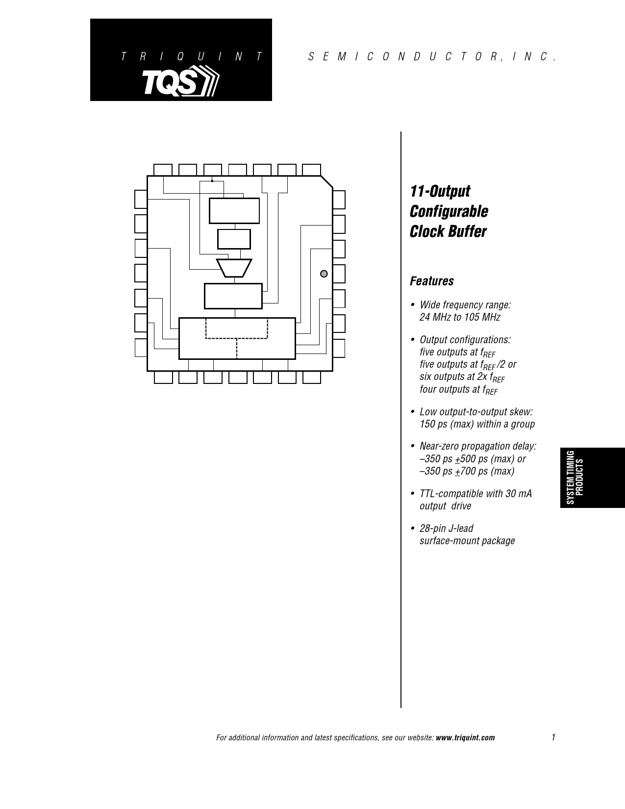
TriQuint’s GA1087 is a configurable clock buffer which generates 11 outputs,
operating over a wide range of frequencies — from 24 MHz to 105 MHz.
The outputs are available at either 1x and 2x or at 1x and 1/2 x the
reference clock frequency, fREF . When one of the Group A outputs
(Q5–Q10) is used as feedback to the PLL, all Group A outputs will be at
fREF , and all Group B outputs (Q0–Q4) will be at 1/2 x fREF . When one of
the Group B outputs is used as feedback to the PLL, all Group A outputs
will be at 2x fREF and all Group B outputs will be at fREF .
A very stable internal Phase-Locked Loop (PLL) provides low-jitter
operation. Completely self-contained, this PLL requires no external
capacitors or resistors. The PLL’s voltage-controlled oscillator (VCO)
has a frequency range from 280 MHz to 420 MHz. By feeding back one
of the output clocks to FBIN, the PLL continuously maintains frequency
and phase synchronization between the reference clock (REFCLK) and
each of the outputs.
TriQuint’s patented output buffer design delivers a very low output-to-
output skew of 150 ps (max). The GA1087’s symmetrical TTL outputs
are capable of sourcing and sinking 30 mA.
GA1087
11-Output
Configurable
Clock Buffer
Features
• Wide frequency range:
24 MHz to 105 MHz
• Output configurations:
five outputs at fREF
five outputs at fREF /2 or
six outputs at 2x fREF
four outputs at fREF
• Low output-to-output skew:
150 ps (max) within a group
• Near-zero propagation delay:
–350 ps +500 ps (max) or
–350 ps +700 ps (max)
• TTL-compatible with 30 mA
output drive
• 28-pin J-lead
surface-mount package
For additional information and latest specifications, see our website: www.triquint.com
1
1 page 
GA1087
AC Characteristics (VDD = +5 V + 5%, TA = 0 °C to +70 °C)
Symbol
t CPWH
t CPWL
t IR
Input Clock (REFCLK)
CLK pulse width HIGH
CLK pulse width LOW
Input rise time (0.8 V - 2.0 V)
Test Conditions (Figure 3) 1
Figure 4
Figure 4
Min
3
3
—
Typ Max Unit
--- — ns
--- — ns
— 2.0 ns
Symbol Input Clock (Q0–Q10)
Test Conditions (Figure 3) 1
Min
t OR,t OF
t PD1 2
t PD2 2
t SKEW1 3
t SKEW2 3
t SKEW3 3
t SKEW4 3
t CYC 4
t JP 5
t JR 5
t SYNC 6
Rise/fall time (0.8 V – 2.0 V)
CLK ↑ to FBIN ↑ (GA1087-MC500)
CLK ↑ to FBIN ↑ (GA1087-MC700)
Rise–rise, fall–fall (within group)
Rise–rise, fall–fall (group-to-group, aligned)
Rise–rise, fall–fall (group-to-group, non-aligned)
Rise–fall, fall–rise
Duty-cycle Variation
Period-to-Period Jitter
Random Jitter
Synchronization Time
Figure 4
Figure 4
Figure 4
Figure 5
Figure 6 (skew2 takes into account skew1)
Figure 7 (skew3 takes into account skews1, 2)
Figure 8 (skew4 takes into account skew3)
Figure 4
Figure 4
Figure 4
350
–850
–1050
—
—
—
—
–1000
—
—
—
Typ
—
–350
–350
60
75
—
—
0
80
190
10
Max
1400
+150
+350
150
350
650
1200
+1000
200
400
500
Unit
ps
ps
ps
ps
ps
ps
ps
ps
ps
ps
µs
Notes: 1. All measurements are tested with a REFCLK having a rise time of 0.5 ns (0.8 V to 2.0 V).
2. The PLL maintains alignment of CLK and FBIN at all times. This specification applies to the rising edge only because
the input duty cycle can vary.
while the output duty cycle is typically 50/50. The delay tPD is measured at the 1.5 V level between CLK and FBIN.
3. Skew specifies the width of the window in which outputs switch, and is measured at 1.5 V.
4. This specification represents the deviation from 50/50 on the outputs.
5. Jitter specifications refer to peak-to-peak value. tJR is the jitter on the output with respect to the reference clock.
tJP is the jitter on the output with respect to the output’s previous rising edge.
6. tSYNC is the time required for the PLL to synchronize; this assumes the presence of a CLK signal and
a connection from one of the outputs to FBIN.
Figure 3. AC Test Circuit
+5 V
R1 Z
R2
+5 V
R1 Z
R2
Notes:
R1 = 160 Ω
R2 = 71 Ω
Y+Z=X
Y
FBIN
CLK
Q0
Q1
Q2
•
•
•
•
Q10
50 Ω
X
•
•
•
•
+5 V
R1 +5 V
R2 R1
R2
+5 V
R1
R2
For additional information and latest specifications, see our website: www.triquint.com
5
5 Page | ||
| Páginas | Total 10 Páginas | |
| PDF Descargar | [ Datasheet GA1087.PDF ] | |
Hoja de datos destacado
| Número de pieza | Descripción | Fabricantes |
| GA1085 | 11-Output Configurable Clock Buffer | TriQuint Semiconductor |
| GA1086 | 11-Output Clock Buffer | TriQuint Semiconductor |
| GA1087 | 11-Output Configurable Clock Buffer | TriQuint Semiconductor |
| GA1088 | 11-Output Configurable Clock Buffer | TriQuint Semiconductor |
| Número de pieza | Descripción | Fabricantes |
| SLA6805M | High Voltage 3 phase Motor Driver IC. |
Sanken |
| SDC1742 | 12- and 14-Bit Hybrid Synchro / Resolver-to-Digital Converters. |
Analog Devices |
|
DataSheet.es es una pagina web que funciona como un repositorio de manuales o hoja de datos de muchos de los productos más populares, |
| DataSheet.es | 2020 | Privacy Policy | Contacto | Buscar |