|
|
|
PDF GP801DDS18 Data sheet ( Hoja de datos )
| Número de pieza | GP801DDS18 | |
| Descripción | Dual Switch Low VCE(SAT) IGBT Module | |
| Fabricantes | Dynex Semiconductor | |
| Logotipo | ||
Hay una vista previa y un enlace de descarga de GP801DDS18 (archivo pdf) en la parte inferior de esta página. Total 10 Páginas | ||
|
No Preview Available !
GP801DDS18
Replaces January 2000 version, DS235-3.0
FEATURES
s Low VCE(SAT)
s Non Punch Through Silicon
s Isolated Copper Baseplate
s Low Inductance Internal Construction
s 800A Per Arm
GP801DDS18
Dual Switch Low VCE(SAT) IGBT Module
DS5235-4.1 January 2001
KEY PARAMETERS
VCES
VCE(sat)
IC
I
C(PK)
(typ)
(max)
(max)
1800V
2.6V
800A
1600A
APPLICATIONS
s High Reliability Inverters
s Motor Controllers
s Traction Drives
s Resonant Converters
12(C2)
2(C2)
7(C1)
4(E2)
1(E1)
11(G2)
10(E2)
3(C1)
5(E1)
6(G1)
The Powerline range of high power modules includes dual
and single switch configurations covering voltages from 600V to
3300V and currents up to 4800A.
The GP801DDS18 is a dual switch 1800V, n channel
enhancement mode, insulated gate bipolar transistor (IGBT)
module. Designed with low VCE(SAT) to minimise conduction
losses, the module is of particular relevance in low to medium
frequency applications. The IGBT has a wide reverse bias safe
operating area (RBSOA) ensuring reliability in demanding
applications.
The module incorporates an electrically isolated base plate
and low inductance construction enabling circuit designers to
optimise circuit layouts and utilise earthed heat sinks for safety.
ORDERING INFORMATION
Order As:
GP801DDS18
Note: When ordering, please use the whole part number.
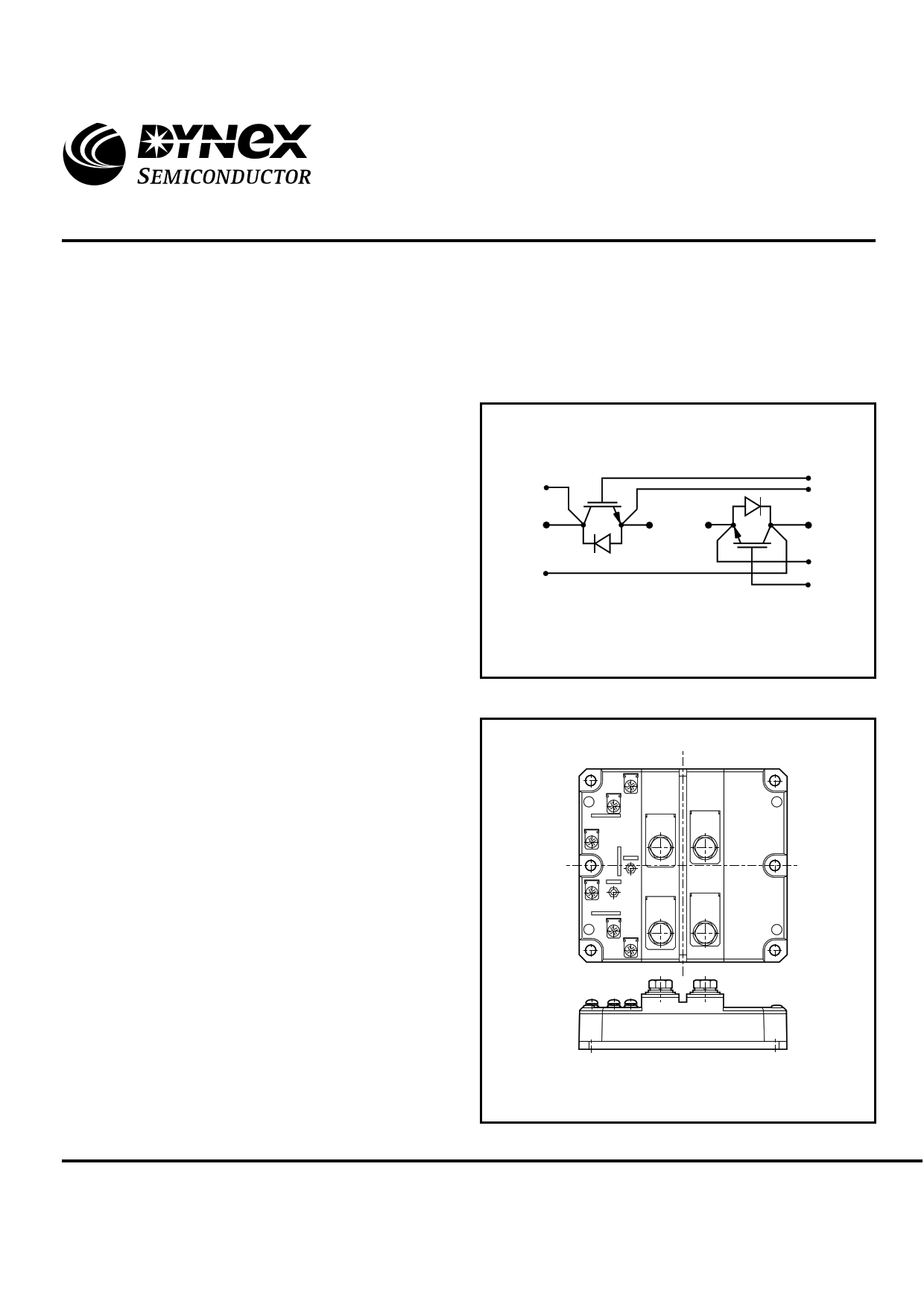
Fig. 1 Dual switch circuit diagram
5
6
7
8
3
9
12
11
10
4
1
2
Outline type code: D
(See package details for further information)
Fig. 2 Electrical connections - (not to scale)
Caution: This device is sensitive to electrostatic discharge. Users should follow ESD handling procedures.
www.dynexsemi.com
1/10
1 page 
GP801DDS18
TYPICAL CHARACTERISTICS
1600
1400
Common emitter
Tcase = 25˚C
Vge = 20/15/12/10V
1200
1000
800
600
400
200
0
0 1.0 2.0 3.0 4.0
Collector-emitter voltage, Vce - (V)
Fig. 3 Typical output characteristics
5.0
1600
1400
Common emitter
Tcase = 125˚C
Vge = 20/15/12/10V
1200
1000
800
600
400
200
0
0 1.0 2.0 3.0 4.0 5.0
Collector-emitter voltage, Vce - (V)
Fig. 4 Typical output characteristics
6.0
1000
900
800
Tcase = 125˚C
VGE = ±15V
VCE = 800V
Rg = 2.2 OhmΩ
700
600 EOFF
500
EON
400
300
200 EREC
100
0
0 100 200 300 400 500 600 700 800
Collector current, IC - (A)
Fig. 5 Typical switching energy vs collector current
1400
1200
Tcase = 125˚C
VGE = ±15V
VCE = 900V
IC = 800A
1000
800
EOFF
EON
600
400
200 EREC
0
0 1 2 3 4 5 6 7 8 9 10
Gate resistance, RG - (Ohms)
Fig. 6 Typical switching energy vs gate resistance
Caution: This device is sensitive to electrostatic discharge. Users should follow ESD handling procedures.
www.dynexsemi.com
5/10
5 Page | ||
| Páginas | Total 10 Páginas | |
| PDF Descargar | [ Datasheet GP801DDS18.PDF ] | |
Hoja de datos destacado
| Número de pieza | Descripción | Fabricantes |
| GP801DDS18 | Dual Switch Low VCE(SAT) IGBT Module | Dynex Semiconductor |
| Número de pieza | Descripción | Fabricantes |
| SLA6805M | High Voltage 3 phase Motor Driver IC. |
Sanken |
| SDC1742 | 12- and 14-Bit Hybrid Synchro / Resolver-to-Digital Converters. |
Analog Devices |
|
DataSheet.es es una pagina web que funciona como un repositorio de manuales o hoja de datos de muchos de los productos más populares, |
| DataSheet.es | 2020 | Privacy Policy | Contacto | Buscar |