|
|
PDF LC75813E Data sheet ( Hoja de datos )
| Número de pieza | LC75813E | |
| Descripción | General-Purpose LCD Driver | |
| Fabricantes | Sanyo Semicon Device | |
| Logotipo | ||
Hay una vista previa y un enlace de descarga de LC75813E (archivo pdf) en la parte inferior de esta página. Total 26 Páginas | ||
|
No Preview Available !
Ordering number : ENN7159
CMOS IC
LC75813E, 75813T
1/3, 1/4 Duty General-Purpose LCD Driver
Overview
The LC75813E and LC75813T are 1/3 duty and 1/4 duty
general-purpose LCD drivers that can be used for
frequency display in electronic tuners under the control of
a microcontroller. The LC75813E and LC75813T can
drive an LCD with up to 344 segments directly. The
LC75813E and LC75813T can also control up to 8
general-purpose output ports. Since the LC75813E and
LC75813T use separate power supply systems for the
LCD drive block and the logic block, the LCD driver
block power-supply voltage can be set to any voltage in
the range 2.7 to 6.0 volts, regardless of the logic block
power-supply voltage.
Specifications
Absolute Maximum Ratings at Ta = 25°C, VSS = 0 V
Features
• Switching between 1/3 duty and 1/4 duty drive
techniques under serial data control.
• Switching between 1/2 bias and 1/3 bias drive
techniques under serial data control.
• Up to 261 segments for 1/3 duty drive and 344 segments
for 1/4 duty drive can be displayed.
• Serial data input supports CCB format communication
with the system controller.
• Serial data control of the power-saving mode based
backup function and all the segments forced off
function.
• Serial data control of switching between the segment
output port and the general-purpose output port
functions.
Parameter
Maximum supply voltage
Input voltage
Output voltage
Output current
Allowable power dissipation
Operating temperature
Storage temperature
Symbol
VDD max
VLCD max
VIN1
VIN2
VIN3
VOUT1
VOUT2
IOUT1
IOUT2
IOUT3
Pd max
Topr
Tstg
Conditions
VDD
VLCD
CE, CL, DI, INH
OSC
VLCD1, VLCD2
OSC
S1 to S87, COM1 to COM4, P1 to P8
S1 to S87
COM1 to COM4
P1 to P8
Ta = 85°C
Ratings
–0.3 to +7.0
–0.3 to +7.0
–0.3 to +7.0
–0.3 to VDD + 0.3
–0.3 to VLCD + 0.3
–0.3 to VDD + 0.3
–0.3 to VLCD + 0.3
300
3
5
200
–40 to +85
–55 to +125
Unit
V
V
V
µA
mA
mW
°C
°C
• CCB is a trademark of SANYO ELECTRIC CO., LTD.
• CCB is SANYO’s original bus format and all the bus
addresses are controlled by SANYO.
Any and all SANYO products described or contained herein do not have specifications that can handle
applications that require extremely high levels of reliability, such as life-support systems, aircraft’s
control systems, or other applications whose failure can be reasonably expected to result in serious
physical and/or material damage. Consult with your SANYO representative nearest you before using
any SANYO products described or contained herein in such applications.
SANYO assumes no responsibility for equipment failures that result from using products at values that
exceed, even momentarily, rated values (such as maximum ratings, operating condition ranges, or other
parameters) listed in products specifications of any and all SANYO products described or contained
herein.
http://semicon.sanyo.com/en/network
20102RM (OT) No. 7159-1/26
1 page 
LC75813E, 75813T
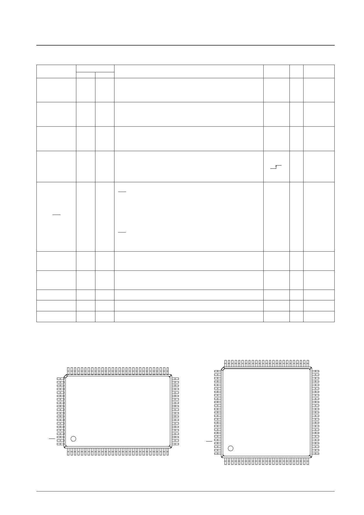
Pin Functions
Symbol
S1/P1 to S8/P8
S9 to S86
Pin No.
LC75813E LC75813T
Function
3 to 10 1 to 8 Segment outputs for displaying the display data transferred by serial data
input. The pins S1/P1 to S8/P8 can be used as general-purpose output
11 to 88 9 to 86 ports when so set up by the control data.
COM1 to COM3
COM4/S87
92 to 90 90 to 88 Common driver outputs.
89 87 The frame frequency is fO Hz.
The COM4/S87 pin can be used as a segment output in 1/3 duty.
OSC
CE
CL
DI
INH
Oscillator connection.
98 96 An oscillator circuit is formed by connecting an external resistor and
capacitor to this pin.
100 98 Serial data transfer inputs. These pins are connected to the control
microprocessor.
1 99 CE: Chip enable
CL: Synchronization clock
2 100 DI: Transfer data
Display off control input
• INH = low (VSS) ....Off
S1/P1 to S8/P8 = low (VSS)
(These pins are forcibly set to the segment output port
99 97
function and fixed at the VSS level.)
S9 to S86 = low (VSS)
COM1 to COM3 = low (VSS)
COM4/S87 = low (VSS)
• INH = high (VDD) ..On
Note that serial data transfers can be performed when the display is forced
off by this pin.
VLCD1
Used to apply the LCD drive 2/3 bias voltage externally. This pin must be
95 93 connected to VLCD2 when 1/2 bias drive is used.
VLCD2
VDD
VLCD
VSS
Used to apply the LCD drive 1/3 bias voltage externally. This pin must be
96 94 connected to VLCD1 when 1/2 bias drive is used.
93 91 Logic block power supply. Provide a voltage in the range 2.7 to 6.0 V.
94 92 LCD driver block power supply. Provide a voltage in the range 2.7 to 6.0 V.
97 95 Ground pin. Connect to ground.
Active
Handling
I/O when unused
— O Open
— O Open
— I/O VDD
HI
I GND
—I
L I GND
— I Open
— I Open
——
——
——
—
—
—
Pin Assignments
80
81
S79
S80
S81
S82
S83
S84
S85
S86
S87/COM4
COM3
COM2
COM1
VDD
VLCD
VLCD1
VLCD2
VSS
OSC
INH
CE
100
1
LC75813E
(QFP100E)
51
50
S48
S47
S46
S45
S44
S43
S42
S41
S40
S39
S38
S37
S36
S35
S34
S33
S32
S31
S30
S29
31
30
75
76
S76
S77
S78
S79
S80
S81
S82
S83
S84
S85
S86
S87/COM4
COM3
COM2
COM1
VDD
VLCD
VLCD1
VLCD2
VSS
OSC
INH
CE
CL
DI
100
1
LC75813T
(TQFP100)
51
50
S50
S49
S48
S47
S46
S45
S44
S43
S42
S41
S40
S39
S38
S37
S36
S35
S34
S33
S32
S31
S30
S29
S28
S27
S26
26
25
Top view
No. 7159-5/26
5 Page 
LC75813E, 75813T
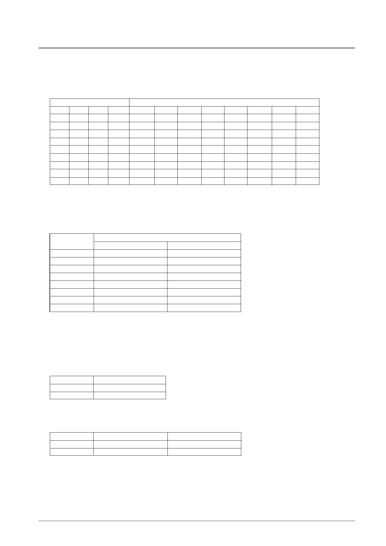
Control Data Functions
1. P0 to P3: Segment output port/general-purpose output port switching control data.
These control data bits switch the S1/P1 to S8/P8 output pins between their segment output port and general-purpose
output port functions.
Control data
P0 P1 P2 P3
00 0 0
00 0 1
00 1 0
00 1 1
01 0 0
01 0 1
01 1 0
01 1 1
10 0 0
S1/P1
S1
P1
P1
P1
P1
P1
P1
P1
P1
S2/P2
S2
S2
P2
P2
P2
P2
P2
P2
P2
Note: Sn (n = 1 to 8): Segment output ports
Pn (n = 1 to 8): General-purpose output ports
S3/P3
S3
S3
S3
P3
P3
P3
P3
P3
P3
Output pin state
S4/P4 S5/P5
S4 S5
S4 S5
S4 S5
S4 S5
P4 S5
P4 P5
P4 P5
P4 P5
P4 P5
S6/P6
S6
S6
S6
S6
S6
S6
P6
P6
P6
S7/P7
S7
S7
S7
S7
S7
S7
S7
P7
P7
S8/P8
S8
S8
S8
S8
S8
S8
S8
S8
P8
Also note that when the general-purpose output port function is selected, the output pins and the display data will
have the correspondences listed in the tables below.
Output pin
S1/P1
S2/P2
S3/P3
S4/P4
S5/P5
S6/P6
S7/P7
S8/P8
Corresponding display data
1/3 duty
1/4 duty
D1 D1
D4 D5
D7 D9
D10 D13
D13 D17
D16 D21
D19 D25
D22 D29
For example, when 1/4 duty drive scheme is used, if the general-purpose output port function is selected for the
S4/P4 output pin, that output pin will output a high level (VLCD) when the display data D13 is 1, and a low level
(VSS) when the D13 is 0.
2. DR: 1/2 bias drive or 1/3 bias drive switching control data
This control data bit selects either 1/2 bias drive or 1/3 bias drive.
DR Bias drive scheme
0 1/3 bias drive
1 1/2 bias drive
3. DT: 1/3 duty drive or 1/4 duty drive switching control data
This control data bit selects either 1/3 duty drive or 1/4 duty drive.
DT Duty drive scheme
0 1/4 duty drive
1 1/3 duty drive
Note: COM4: common output
S87: segment output
Output pin state (COM4/S87)
COM4
S87
No. 7159--11/26
11 Page | ||
| Páginas | Total 26 Páginas | |
| PDF Descargar | [ Datasheet LC75813E.PDF ] | |
Hoja de datos destacado
| Número de pieza | Descripción | Fabricantes |
| LC75813E | General-Purpose LCD Driver | Sanyo Semicon Device |
| LC75813E | General-Purpose LCD Driver | ON Semiconductor |
| LC75813T | General-Purpose LCD Driver | Sanyo Semicon Device |
| LC75813T | General-Purpose LCD Driver | ON Semiconductor |
| Número de pieza | Descripción | Fabricantes |
| SLA6805M | High Voltage 3 phase Motor Driver IC. |
Sanken |
| SDC1742 | 12- and 14-Bit Hybrid Synchro / Resolver-to-Digital Converters. |
Analog Devices |
|
DataSheet.es es una pagina web que funciona como un repositorio de manuales o hoja de datos de muchos de los productos más populares, |
| DataSheet.es | 2020 | Privacy Policy | Contacto | Buscar |
