|
|
|
PDF LC78626 Data sheet ( Hoja de datos )
| Número de pieza | LC78626 | |
| Descripción | DSP for Compact Disk Players | |
| Fabricantes | Sanyo Semicon Device | |
| Logotipo | ||
Hay una vista previa y un enlace de descarga de LC78626 (archivo pdf) en la parte inferior de esta página. Total 30 Páginas | ||
|
No Preview Available !
Ordering number : EN5692
CMOS LSI
LC78626E
DSP for Compact Disk Players
Overview
The LC78626E is a monolithic compact disk player signal
processing and servo control CMOS IC equipped with an
internal anti-shock control function. Designed for total
functionality including support for EFM-PLL, and one-bit
D/A converter, and containing analog low-pass filter, the
LC78626E provides optimal cost-performance for low-end
CD players that provide anti-shock systems. The basic
functions provided by this IC include modulation of the
EFM signal from the optical pick-up, deinterleaving,
detection and correction of signal errors, prevention of a
maximum of approximately 10 seconds of skipping, signal
processing such as digital filtering (which is useful in
reducing the cost of the player), and processing of a
variety of servo-related commands from the
microprocessor.
Functions
• When an HF signal is input, it is sliced to precise levels
and converted to an EFM signal. The phase is compared
with the internal VCO and a PLL clock is reproduced at
an average frequency of 4.3218 MHz.
• Precise timing for a variety of required internal timing
needs (including the generation of the reference clock) is
produced by the attachment of an external 16.9344 MHz
crystal oscillator.
• The speed of revolution of the disk motor is controlled
by the frame phase difference signal generated by the
playback clock and the reference clock.
• The frame synchronizing signal is detected, stored, and
interpolated to insure stable data read back.
• The EFM signal is demodulated and converted to 8-bit
symbolic data.
• The demodulated EFM signal is divided into subcodes
and output to the external microprocessor. (Three
general I/O ports are shared [exclusively] for this
purpose.)
• After the subcode Q signal passes the CRC check, it is
output to the microprocessor through a serial
transmission (LSB first).
• The demodulated EFM signal is buffered in the internal
RAM, which is able to absorb ± 4 frame's worth of jitter
resulting from variations in the disk rotation speed.
• The demodulated EFM signal is unscrambled to a
specific sequence, and deinterleaving is performed.
• Error detection and correction is performed, as is a flag
process. (C1: two error/C2: two error correction
method.)
• The C2 flag is set after referencing the C1 flag and the
results of the C2 check, where the signal from the C2
flag is interpolated or held at its previous level. The
interpolation circuit uses double interpolation. When
there are two or more C2 flags in a row, the previous
value is held.
Continued on next page.
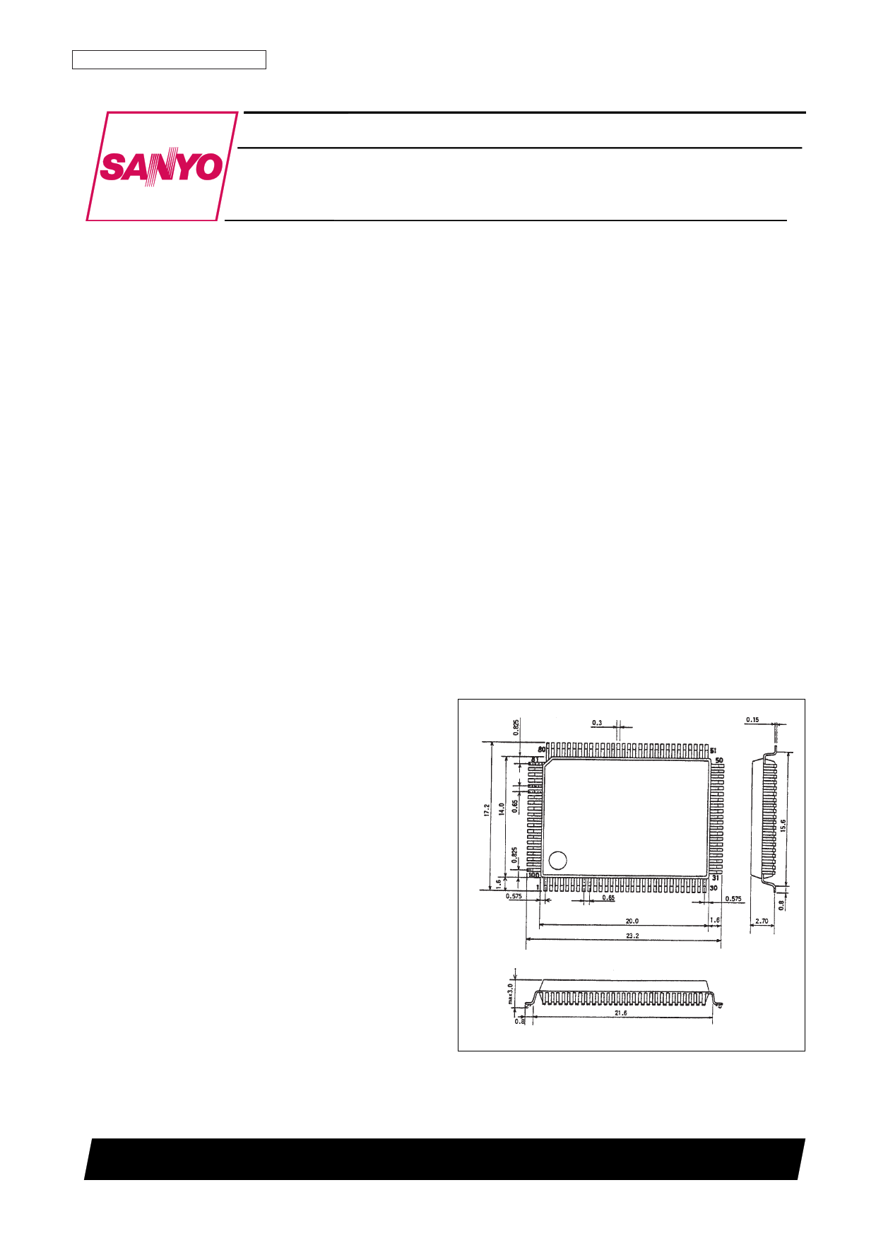
Package Dimensions
unit: mm
3151-QFP100E (FLP100)
[LC78626E]
SANYO: QIP100E (FLP100)
SANYO Electric Co.,Ltd. Semiconductor Bussiness Headquarters
TOKYO OFFICE Tokyo Bldg., 1-10, 1 Chome, Ueno, Taito-ku, TOKYO, 110-0005 JAPAN
13098HA(OT) No. 5692-1/32
1 page 
LC78626E
Specifications
Absolute Maximum Ratings at Ta = 25°C, VSS = 0V
Parameter
Maximum power supply voltage
Input voltage
Output voltage
Allowable power dissipation
Operating temperature range
Storage temperature range
Symbol
VDD max
VIN
VOUT
Pd max
Topr
Tstg
Conditions
Allowable Operating Range at Ta = 25°C, VSS = 0V
Parameter
Power supply voltage
Input high level voltage
Input low level voltage
Data setup time
Data hold time
High level clock pulse width
Low level clock pulse width
Data read access time
Command transfer time
Subcode Q read enable time
Subcode ready cycle time
Subcode read enable time
Port input data setup time
Port input data hold time
Port input clock setup time
Port output data delay time
Input level
Range of operating frequencies
Crystal oscillator frequency
Symbol
Conditions
VDD1
VDD2
VIH1
VIH2
VIH3
VIL1
VIL2
VIL2
tSU
tHD
tWH
tWL
tRAC
tRWC
tSQE
tSC
tSE
tCSU
tCHD
tRCQ
tCDD
VIN1
VIN2
fOP
fX
VDD, XVDD, LVDD, RVDD, VVDD:
ATT/DF/DAC to the normal speed
VDD, XVDD, LVDD, RVDD, VVDD:
All functions guaranteed to 2× speed
I/O and input pins with the exception of
EFMI and DRAM0 to DRAM3
EFMI
DRAM0 to DRAM3
I/O and input pins with the exception of
EFMI and DRAM0 to DRAM3
EFMI
DRAM0 to DRAM3
COIN, RWC: Figure 1
COIN, RWC: Figure 1
SBCK, CQCK: Figures 1 to 3
SBCK, CQCK: Figures 1 to 3
SQOUT, PW: Figures 2 and 3
RWC: Figure 1
WRQ: Figure 2, no RWC signal
SFSY: Figure 3
SFSY: Figure 3
CONT2 to CONT5, RWC: Figure 4
CONT2 to CONT5, RWC: Figure 4
RWC, CQCK: Figure 4
CONT2 TO CONT5, RWC: Figure 5
EFMI: slice level control, VDD = 3.0 V
XIN: C coupling input
EFMI
XIN, XOUT
Ratings
VSS–0.3 to VSS+7.0
VSS–0.3 to VDD+0.3
VSS–0.3 to VDD+0.3
400
–20 to +75
–40 to +125
Unit
V
V
V
mW
°C
°C
min
3.0
Ratings
typ
max
5.5
Unit
V
3.6 5.5 V
0.7VDD
0.6VDD
0.45VDD
0
0
0
400
400
400
400
0
1000
400
400
400
100
11.2
136
0.8
1.0
16.9344
VDD
VDD
VDD
0.3VDD
0.4VDD
0.2VDD
400
1200
10
V
V
V
V
V
V
ns
ns
ns
ns
ns
ns
ms
µs
µs
ns
ns
ns
ns
Vp-p
Vp-p
MHz
MHz
Electrical Characteristics at Ta = 25°C, VDD = 3.2 V VSS = 0V
Parameter
Consumption current
Input high level current.
Symbol
Conditions
IDD
VDD, XVDD, LVDD, RVDD, VVDD:
VDD = 3.0 to 3.4 V with normal playback
DEFI, EFMI, HFL, TES, RWC, COIN, CQCK,
FMT, MR1, RES, TESD, WOK, PAUSE IN,
IIH1 SHOCK, TESCLK, TESA, TESB, TESC,
TESGB, TEST1: VIN = VDD
TAI, TEST2 to TEST5, CS, TESE:
IIH2 VIN = VDD = 3.4 V
Ratings
Unit
min typ max
14 20 mA
5 µA
15 55 µA
Continued on next page.
No. 5692-5/32
5 Page 
LC78626E
Continued from preceding page.
PIn Pin
No. Name
70 MMC0
71 MMC1
72 MMC2
73 MMC3
74 OVF
75 CNTOK
76 WOK
77 PAUSE IN
78 NGJ
79 EMPN
80 SHOCK
81 DRAM3
82 DRAM2
83 DRAM1
84 DRAM0
85 OE
86 WE
87 CAS
88 RAS
89 AD9
90 AD8
91 AD7
92 AD6
93 AD5
94 VSS
95 AD4
96 AD3
97 AD2
98 AD1
99 AD0
100 VDD
I/O Description
O Remaining DRAM output.
O Remaining DRAM output.
O Remaining DRAM output.
O Remaining DRAM output.
O DRAM write terminated. (An RZP pulse is output when there is an overflow or a shock.)
O Data contact point detection complete signal: low→ high: detection complete. (DRAM write start).
I DRAM write enable signal input: high: write enable.
I Pause signal input: high: pause.
O C2F data contact point detection start signal: low → high: detection start.
O Remaining DRAM alarm output: low: memory low.
I C2F shock detect pause signal input: low: pause shock detection.
I/O DRAM data bus
I/O DRAM data bus
I/O DRAM data bus
I/O DRAM data bus
O DRAM control signal.
O DRAM control signal.
O DRAM control signal.
O DRAM control signal.
O DRAM address bus
O DRAM address bus
O DRAM address bus
O DRAM address bus
O DRAM address bus
P Digital system ground. Must be connected to 0 V.
O DRAM address bus
O DRAM address bus
O DRAM address bus
O DRAM address bus
O DRAM address bus
P Digital system power supply.
No. 5692-11/32
11 Page | ||
| Páginas | Total 30 Páginas | |
| PDF Descargar | [ Datasheet LC78626.PDF ] | |
Hoja de datos destacado
| Número de pieza | Descripción | Fabricantes |
| LC78620E | Compact Disc Player DSP | Sanyo Semicon Device |
| LC78621E | Compact Disc Player DSP | Sanyo Semicon Device |
| LC78622E | Compact Disc Player DSP | Sanyo Semicon Device |
| LC78622NE | Compact Disc Player DSP | Sanyo Semicon Device |
| Número de pieza | Descripción | Fabricantes |
| SLA6805M | High Voltage 3 phase Motor Driver IC. |
Sanken |
| SDC1742 | 12- and 14-Bit Hybrid Synchro / Resolver-to-Digital Converters. |
Analog Devices |
|
DataSheet.es es una pagina web que funciona como un repositorio de manuales o hoja de datos de muchos de los productos más populares, |
| DataSheet.es | 2020 | Privacy Policy | Contacto | Buscar |