|
|
|
PDF STB7N52K3 Data sheet ( Hoja de datos )
| Número de pieza | STB7N52K3 | |
| Descripción | N-channel Power MOSFET | |
| Fabricantes | STMicroelectronics | |
| Logotipo | ||
Hay una vista previa y un enlace de descarga de STB7N52K3 (archivo pdf) en la parte inferior de esta página. Total 15 Páginas | ||
|
No Preview Available !
STB7N52K3 - STD7N52K3
STF7N52K3 - STP7N52K3
N-channel 525 V, 0.84 Ω, 6.3 A, D2PAK, DPAK, TO-220FP, TO-220
SuperMESH3™ Power MOSFET
Preliminary Data
Features
Type
VDSS
RDS(on)
max
ID
Pw
STB7N52K3
STD7N52K3
STF7N52K3
STP7N52K3
525 V
525 V
525 V
525 V
< 0.98 Ω 6.3 A 90 W
< 0.98 Ω 6.3 A 90 W
< 0.98 Ω 6.3 A(1) 25 W
< 0.98 Ω 6.3 A 90 W
1. Limited by package
■ 100% avalanche tested
■ Extremely high dv/dt capability
■ Gate charge minimized
■ Very low intrinsic capacitances
■ Improved diode reverse recovery
characteristics
■ Zener-protected
Application
■ Switching applications
www.DataSDheeets4Uc.croimption
The new SuperMESH3™ series is obtained
through the combination of a further fine tuning of
ST's well established strip-based PowerMESH™
layout with a new optimization of the vertical
structure. In addition to reducing on-resistance
significantly versus previous generation, special
attention has been taken to ensure a very good
dv/dt capability and higher margin in breakdown
voltage for the most demanding application.
Table 1. Device summary
Order codes
Marking
STB7N52K3
STD7N52K3
STF7N52K3
STP7N52K3
7N52K3
7N52K3
7N52K3
7N52K3
3
1
D²PAK
3
1
DPAK
3
2
1
TO-220
3
2
1
TO-220FP
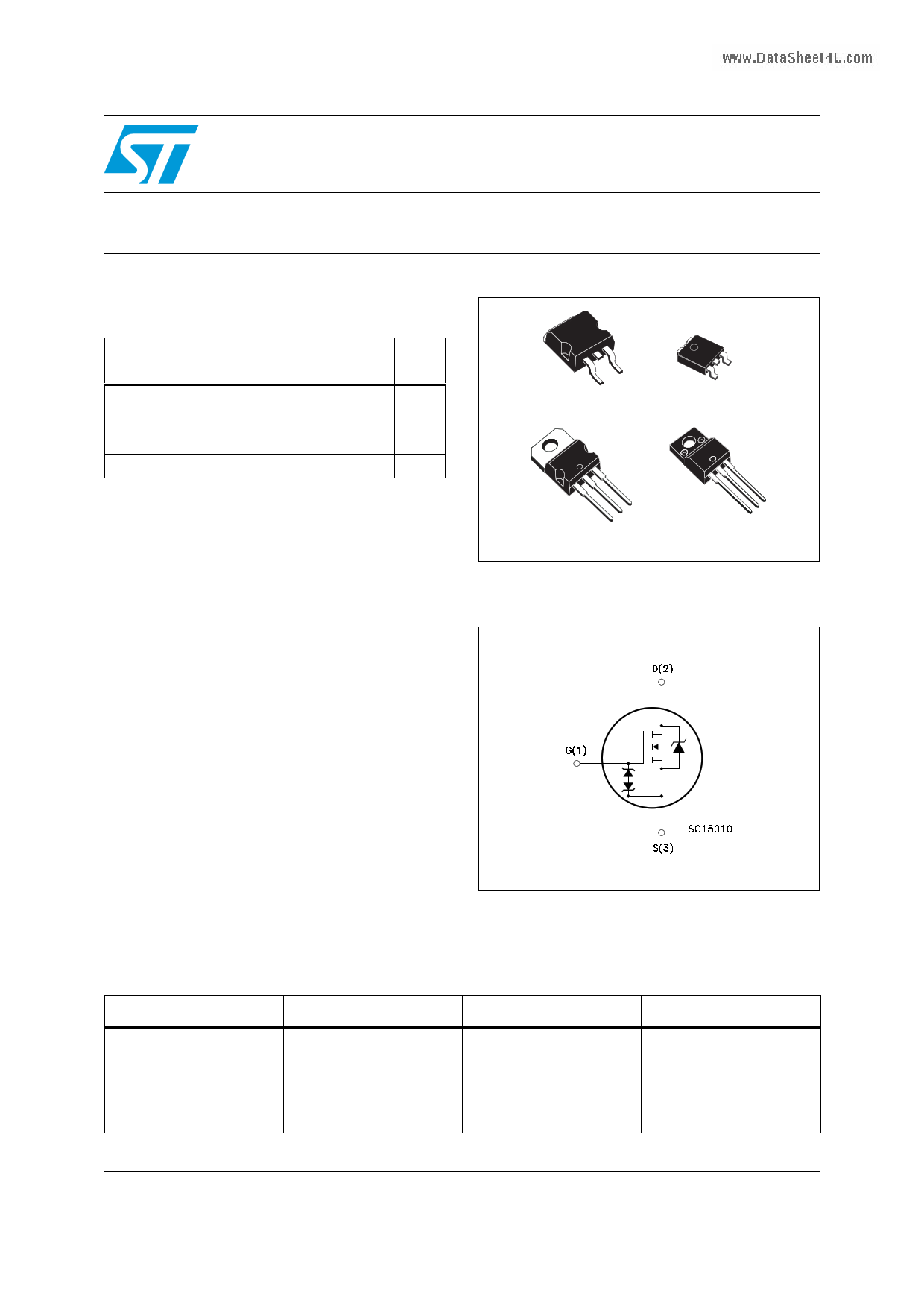
Figure 1. Internal schematic diagram
Package
D²PAK
DPAK
TO-220FP
TO-220
Packaging
Tape and reel
Tape and reel
Tube
Tube
July 2008
Rev 1
This is preliminary information on a new product now in development or undergoing evaluation. Details are subject to
change without notice.
1/15
www.st.com
15
1 page 
STB7N52K3 - STD7N52K3 - STF7N52K3 - STP7N52K3
Electrical characteristics
Table 8.
Symbol
Source drain diode
Parameter
Test conditions
Min. Typ. Max. Unit
ISD
ISDM (1)
VSD (2)
Source-drain current
Source-drain current (pulsed)
Forward on voltage
ISD = 6.3 A, VGS = 0
trr
Qrr
IRRM
Reverse recovery time
Reverse recovery charge
Reverse recovery current
ISD = 6.3 A, di/dt = 100 A/µs
VDD = 30 V (see Figure 7)
trr
Qrr
IRRM
Reverse recovery time
Reverse recovery charge
Reverse recovery current
ISD = 6.3 A, di/dt = 100 A/µs
VDD = 30 V, Tj = 150 °C
(see Figure 7)
1. Pulse width limited by safe operating area
2. Pulsed: Pulse duration = 300 µs, duty cycle 1.5%
6.3 A
25 A
1.6 V
TBD
TBD
TBD
ns
nC
A
TBD
TBD
TBD
ns
nC
A
Table 9.
Symbol
Gate-source Zener diode
Parameter
Test conditions
Min Typ Max Unit
BVGSO(1)
Gate-source breakdown
voltage
Igs=± 1 mA (open drain)
30
V
1. The built-in back-to-back Zener diodes have specifically been designed to enhance not only the device’s
ESD capability, but also to make them safely absorb possible voltage transients that may occasionally be
applied from gate to source. In this respect the Zener voltage is appropriate to achieve an efficient and
cost-effective intervention to protect the device’s integrity. These integrated Zener diodes thus avoid the
usage of external components
www.DataSheet4U.com
5/15
5 Page 
STB7N52K3 - STD7N52K3 - STF7N52K3 - STP7N52K3
Package mechanical data
DIM.
A
A1
A2
b
b4
c
c2
D
D1
E
E1
e
e1
H
L
L1
L2
L4
R
V2
TO-252 (DPAK) mechanical data
min.
2.20
0.90
0.03
0.64
5.20
0.45
0.48
6.00
6.40
4.40
9.35
1
0.60
0o
mm.
typ
5.10
4.70
2.28
2.80
0.80
0.20
max.
2.40
1.10
0.23
0.90
5.40
0.60
0.60
6.20
6.60
4.60
10.10
1
8o
www.DataSheet4U.com
0068772_G
11/15
11 Page | ||
| Páginas | Total 15 Páginas | |
| PDF Descargar | [ Datasheet STB7N52K3.PDF ] | |
Hoja de datos destacado
| Número de pieza | Descripción | Fabricantes |
| STB7N52K3 | N-channel Power MOSFET | STMicroelectronics |
| Número de pieza | Descripción | Fabricantes |
| SLA6805M | High Voltage 3 phase Motor Driver IC. |
Sanken |
| SDC1742 | 12- and 14-Bit Hybrid Synchro / Resolver-to-Digital Converters. |
Analog Devices |
|
DataSheet.es es una pagina web que funciona como un repositorio de manuales o hoja de datos de muchos de los productos más populares, |
| DataSheet.es | 2020 | Privacy Policy | Contacto | Buscar |