|
|
|
PDF GP20B60PD Data sheet ( Hoja de datos )
| Número de pieza | GP20B60PD | |
| Descripción | IRGP20B60PD | |
| Fabricantes | IRF | |
| Logotipo | ||
 1. - IR ( PDF ) Hay una vista previa y un enlace de descarga de GP20B60PD (archivo pdf) en la parte inferior de esta página. Total 10 Páginas | ||
|
No Preview Available !
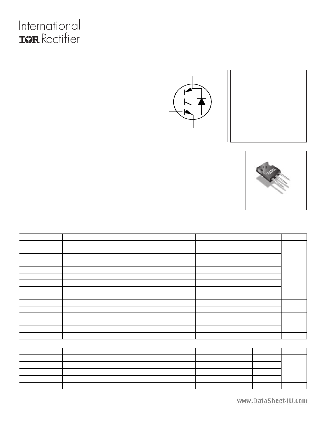
SMPS IGBT
WARP2 SERIES IGBT WITH
ULTRAFAST SOFT RECOVERY DIODE
www.datasheet4u.com
Applications
• Telecom and Server SMPS
• PFC and ZVS SMPS Circuits
• Uninterruptable Power Supplies
• Consumer Electronics Power Supplies
Features
• NPT Technology, Positive Temperature Coefficient
• Lower VCE(SAT)
• Lower Parasitic Capacitances
• Minimal Tail Current
• HEXFRED Ultra Fast Soft-Recovery Co-Pack Diode
• Tighter Distribution of Parameters
• Higher Reliability
C
G
E
n-channel
Benefits
• Parallel Operation for Higher Current Applications
• Lower Conduction Losses and Switching Losses
• Higher Switching Frequency up to 150kHz
PD - 94626
IRGP20B60PD
VCES = 600V
VCE(on) typ. = 2.05V
@ VGE = 15V IC = 13.0A
Equivalent MOSFET
Parameters
RCE(on) typ. = 158mΩ
ID (FET equivalent) = 20A
E
C
G
TO-247AC
Absolute Maximum Ratings
Parameter
VCES
IC @ TC = 25°C
IC @ TC = 100°C
ICM
ILM
IF @ TC = 25°C
IF @ TC = 100°C
IFRM
VGE
PD @ TC = 25°C
PD @ TC = 100°C
TJ
TSTG
Collector-to-Emitter Voltage
Continuous Collector Current
Continuous Collector Current
Pulse Collector Current (Ref. Fig. C.T.4)
dClamped Inductive Load Current
Diode Continous Forward Current
Diode Continous Forward Current
eMaximum Repetitive Forward Current
Gate-to-Emitter Voltage
Maximum Power Dissipation
Maximum Power Dissipation
Operating Junction and
Storage Temperature Range
Soldering Temperature, for 10 sec.
Mounting Torque, 6-32 or M3 Screw
Thermal Resistance
Parameter
RθJC (IGBT)
Thermal Resistance Junction-to-Case-(each IGBT)
RθJC (Diode)
Thermal Resistance Junction-to-Case-(each Diode)
RθCS
Thermal Resistance, Case-to-Sink (flat, greased surface)
RθJA Thermal Resistance, Junction-to-Ambient (typical socket mount)
Weight
Max.
600
40
22
80
80
31
12
42
±20
220
86
-55 to +150
300 (0.063 in. (1.6mm) from case)
10 lbf·in (1.1 N·m)
Min.
–––
–––
–––
–––
–––
Typ.
–––
–––
0.24
–––
6 (0.21)
Max.
0.58
2.5
–––
40
–––
Units
V
A
V
W
°C
Units
°C/W
g (oz)
1 www.irf.com
02/06/03
1 page 
250
200
www.datasheet4u.com
150
EON
EOFF
IRGP20B60PD
1000
tdOFF
100
tdON
10 tF
100
tR
50
0
5 10 15 20 25 30 35
RG (Ω)
Fig. 13 - Typ. Energy Loss vs. RG
TJ = 125°C; L = 200µH; VCE = 390V, ICE = 13A; VGE = 15V
Diode clamp used: 8ETH06 (See C.T.3)
18
16
14
12
10
8
6
4
2
0
0 100 200 300 400 500 600 700
VCE (V)
Fig. 15- Typ. Output Capacitance
Stored Energy vs. VCE
16
14
400V
12
10
8
6
4
2
0
0 10 20 30 40 50 60 70 80
Q G, Total Gate Charge (nC)
Fig. 17 - Typical Gate Charge vs. VGE
ICE = 13A
www.irf.com
1
0 10 20 30 40
RG (Ω)
Fig. 14 - Typ. Switching Time vs. RG
TJ = 125°C; L = 200µH; VCE = 390V, ICE = 13A; VGE = 15V
Diode clamp used: 8ETH06 (See C.T.3)
10000
1000
Cies
Coes
100
Cres
10
1
0
20 40 60 80 100
VCE (V)
Fig. 16- Typ. Capacitance vs. VCE
VGE= 0V; f = 1MHz
1.6
1.5
1.4
1.3
1.2
1.1
1
0.9
0.8
0.7
0.6
-50 0 50 100 150 200
TJ, Junction Temperature (°C)
Fig. 18 - Normalized Typical VCE(on) vs. Junc-
tion Temperature
ICE = 13A, VGE = 15V
5
5 Page | ||
| Páginas | Total 10 Páginas | |
| PDF Descargar | [ Datasheet GP20B60PD.PDF ] | |
Hoja de datos destacado
| Número de pieza | Descripción | Fabricantes |
| GP20B60PD | IRGP20B60PD | IRF |
| Número de pieza | Descripción | Fabricantes |
| SLA6805M | High Voltage 3 phase Motor Driver IC. |
Sanken |
| SDC1742 | 12- and 14-Bit Hybrid Synchro / Resolver-to-Digital Converters. |
Analog Devices |
|
DataSheet.es es una pagina web que funciona como un repositorio de manuales o hoja de datos de muchos de los productos más populares, |
| DataSheet.es | 2020 | Privacy Policy | Contacto | Buscar |