|
|
|
PDF IRF7402 Data sheet ( Hoja de datos )
| Número de pieza | IRF7402 | |
| Descripción | HEXFET Power MOSFET | |
| Fabricantes | International Rectifier | |
| Logotipo | ||
Hay una vista previa y un enlace de descarga de IRF7402 (archivo pdf) en la parte inferior de esta página. Total 8 Páginas | ||
|
No Preview Available !
PD - 93851A
www.datasheet4u.com
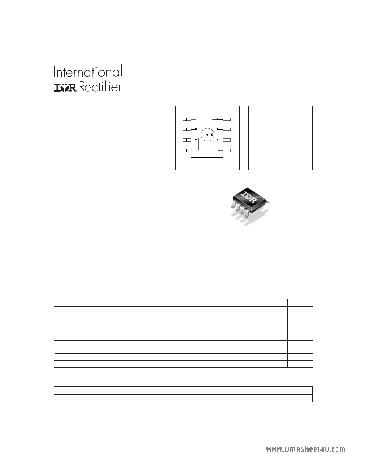
IRF7402
l Generation V Technology
l Ultra Low On-Resistance
l N-Channel MOSFET
l Very Small SOIC Package
l Low Profile (<1.1mm)
l Available in Tape & Reel
l Fast Switching
S
S
S
G
Description
Fifth Generation HEXFET® power MOSFETs from
International Rectifier utilize advanced processing
techniques to achieve extremely low on-resistance per
silicon area. This benefit, combined with the fast switching
speed and ruggedized device design that HEXFET
power MOSFETs are well known for, provides the
designer with an extremely efficient and reliable device
for use in a wide variety of applications.
HEXFET® Power MOSFET
A
A
1 8D
2 7 D VDSS = 20V
3 6D
4
5D
RDS(on) = 0.035Ω
T op V iew
The SO-8 has been modified through a customized
leadframe for enhanced thermal characterstics and
multiple-die capability making it ideal in a variety of
power applications. With these improvements, multiple
devices can be used in an application with dramatically
reduced board space. The package is designed for
vapor phase, infrared or wave soldering techniques.
Power dissipation of greater than 0.8 W is possible in a
typical PCB mount application.
Absolute Maximum Ratings
ID @ TA = 25°C
ID @ TA = 70°C
IDM
PD @TA = 25°C
PD @TA = 70°C
VGS
dv/dt
TJ, TSTG
Parameter
Continuous Drain Current, VGS @ 4.5V
Continuous Drain Current, VGS @ 4.5V
Pulsed Drain Current
Power Dissipation
Power Dissipation
Linear Derating Factor
Gate-to-Source Voltage
Peak Diode Recovery dv/dt
Junction and Storage Temperature Range
SO-8
Max.
6.8
5.4
54
2.5
1.6
0.02
± 12
5.0
-55 to + 150
Units
A
W
W/°C
V
V/ns
°C
Thermal Resistance
RθJA
Parameter
Maximum Junction-to-Ambient
Max.
50
Units
°C/W
www.irf.com
1
2/22/00
1 page 
www.datasheet4u.com
8.0
6.0
4.0
2.0
0.0
25
50 75 100 125
TC , Case Temperature ( °C)
150
Fig 9. Maximum Drain Current Vs.
Ambient Temperature
IRF7402
VDS
VGS
RG
RD
D.U.T.
4.5V
Pulse Width ≤ 1 µs
Duty Factor ≤ 0.1 %
+
-
V
D
D
Fig 10a. Switching Time Test Circuit
VDS
90%
10%
VGS
td(on) tr
td(off) tf
Fig 10b. Switching Time Waveforms
100
D = 0.50
10 0.20
0.10
0.05
0.02
1
0.01
0.1
0.00001
P DM
t1
t2
SINGLE PULSE
(THERMAL RESPONSE)
0.0001
0.001
Notes:
1. Duty factor D = t1 / t 2
2. Peak TJ = P DM x ZthJC + TC
0.01
0.1
1
t1, Rectangular Pulse Duration (sec)
10
100
Fig 11. Maximum Effective Transient Thermal Impedance, Junction-to-Ambient
www.irf.com
5
5 Page | ||
| Páginas | Total 8 Páginas | |
| PDF Descargar | [ Datasheet IRF7402.PDF ] | |
Hoja de datos destacado
| Número de pieza | Descripción | Fabricantes |
| IRF740 | N-CHANNEL 400V, 10A, Power MOSFET, TO-220 | STMicroelectronics |
| IRF740 | 10A/ 400V/ 0.550 Ohm/ N-Channel Power MOSFET | Intersil Corporation |
| IRF740 | N-Channel Power MOSFETs/ 10A/ 350V/400V | Fairchild Semiconductor |
| IRF740 | N-Channel Power MOSFETs | ART CHIP |
| Número de pieza | Descripción | Fabricantes |
| SLA6805M | High Voltage 3 phase Motor Driver IC. |
Sanken |
| SDC1742 | 12- and 14-Bit Hybrid Synchro / Resolver-to-Digital Converters. |
Analog Devices |
|
DataSheet.es es una pagina web que funciona como un repositorio de manuales o hoja de datos de muchos de los productos más populares, |
| DataSheet.es | 2020 | Privacy Policy | Contacto | Buscar |