|
|
|
PDF GFU30N03 Data sheet ( Hoja de datos )
| Número de pieza | GFU30N03 | |
| Descripción | N-Channel Enhancement Mode MOSFET | |
| Fabricantes | General Semiconductor | |
| Logotipo | ||
Hay una vista previa y un enlace de descarga de GFU30N03 (archivo pdf) en la parte inferior de esta página. Total 5 Páginas | ||
|
No Preview Available !
New Product
GFU30N03
Vishay Semiconductor
www.DataSheet4U.com
N-Channel Enhancement-Mode MOSFET
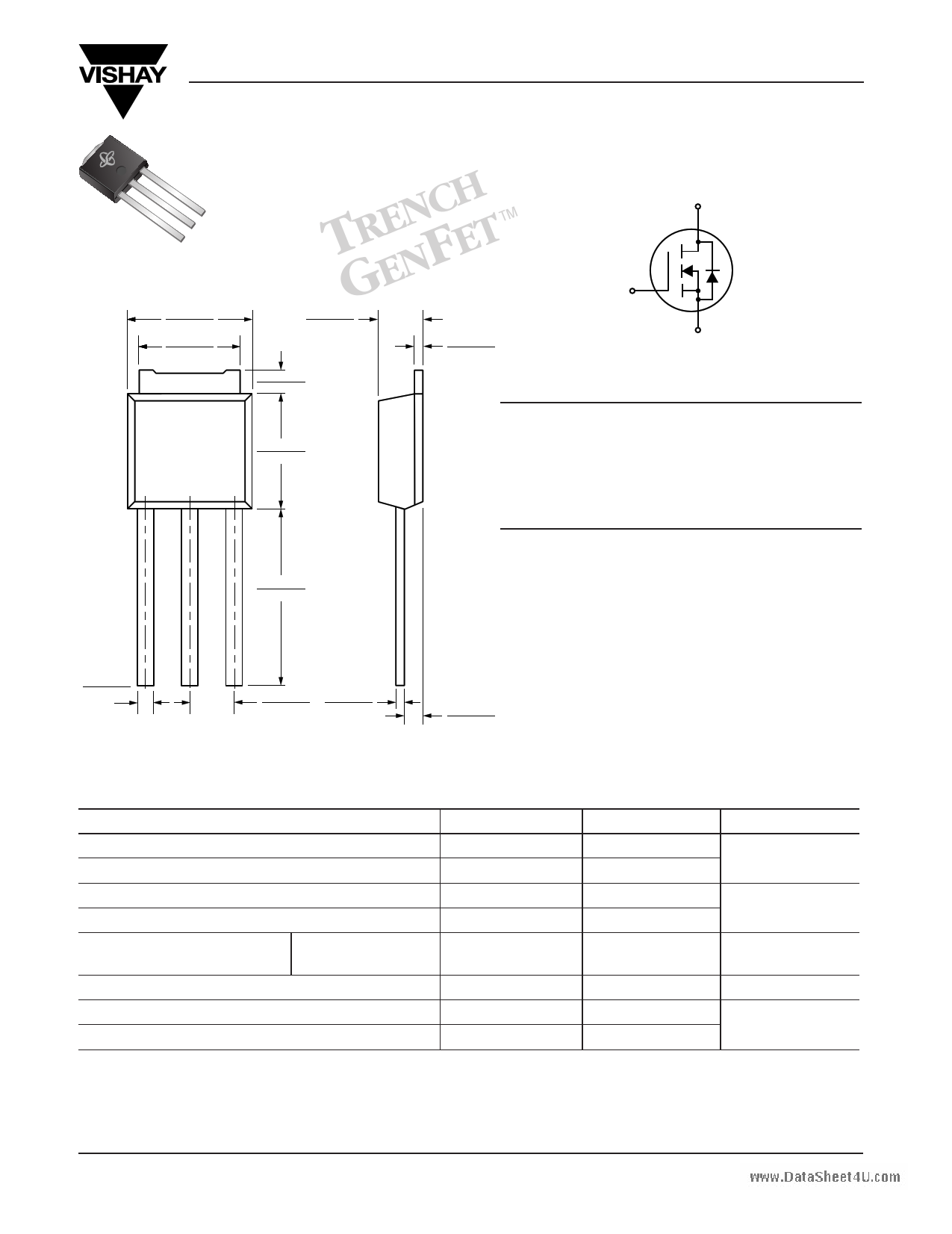
TG FTO-251 (IPAK)
REENNCHETTM
0.265 (6.73)
0.255 (6.48)
0.214 (5.43)
0.206 (5.23)
D
0.094 (2.39)
0.087 (2.21)
0.050 (1.27)
0.035 (0.89)
0.023 (0.58)
0.018 (0.46)
Features
G
D
S
VDS 30V
RDS(ON) 15mΩ
ID 43A
0.245 (6.22)
0.235 (5.97)
GS
• Advanced Trench Process Technology
• High Density Cell Design for Ultra Low On-Resistance
• Specially Designed for Low Voltage DC/DC Converters
and motor drives
• Fast Switching for High Efficiency
Mechanical Data
0.375 (9.53)
0.350 (8.89)
Case: JEDEC TO-251 molded plastic body
Terminals: Solder plated, solderable per
MIL-STD-750, Method 2026
High temperature soldering guaranteed:
250°C/10 seconds at terminals
Weight: 0.011oz., 0.4g
0.035 (0.89)
0.028 (0.71)
0.102 (2.59) 0.023 (0.58)
0.078 (1.98) 0.018 (0.46)
Dimensions in inches and (millimeters)
0.045 (1.14)
0.035 (0.89)
Maximum Ratings and Thermal Characteristics (TC = 25°C unless otherwise noted)
Parameter
Symbol
Limit
Drain-Source Voltage
VDS 30
Gate-Source Voltage
Continuous Drain Current(1)
VGS
ID
± 20
43
Pulsed Drain Current
IDM 80
Maximum Power Dissipation
TC = 25°C
TC = 100°C
PD
44.5
17.8
Operating Junction and Storage Temperature Range
TJ, Tstg
–55 to 150
Junction-to-Case Thermal Resistance
Junction-to-Ambient Thermal Resistance(2)
RθJC
RθJA
2.8
125
Note: (1) Maximum DC current limited by the package
(2) 1-in2 2oz. Cu PCB mounted
Unit
V
A
W
°C
°C/W
Document Number 74573
17-Dec-01
www.vishay.com
1
1 page 
Ratings and
Characteristic Curves (TA = 25°C unless otherwise noted)
GFU30N03
Vishay Semiconductor
Fig. 10 – Breakdown Voltage
vs. Junction Temperature
43
42 ID = 250µA
41
www.DataSheet4U.co4m0
39
38
37
36
--50 --25 0 25 50 75 100 125 150
TJ -- Junction Temperature (°C)
Fig. 12 – Power vs. Pulse Duration
1000
800
600
400
200
0
0.0001 0.001
0.01
0.1
1
10
Fig. 11 – Transient Thermal
Impedance
1. Duty Cycle, D = t1/ t2
2. RθJA(t) = RθJA(norm) *RθJA
3. RθJA = 2.0°C/W
4. TJ --TA = PDM* RθJA(t)
Pulse Duration (sec.)
Fig. 13 – Maximum Safe Operating Area
1000
100
RDS(ON) Limit
10
VGS = 10V
Single Pulse
RθJC = 2.0°C/W
TA = 25°C
1
0.1 1
DC
100µs
10ms1ms
10
VDS -- Drain-Source Voltage (V)
100
Document Number 74573
17-Dec-01
www.vishay.com
5
5 Page | ||
| Páginas | Total 5 Páginas | |
| PDF Descargar | [ Datasheet GFU30N03.PDF ] | |
Hoja de datos destacado
| Número de pieza | Descripción | Fabricantes |
| GFU30N03 | N-Channel Enhancement Mode MOSFET | General Semiconductor |
| Número de pieza | Descripción | Fabricantes |
| SLA6805M | High Voltage 3 phase Motor Driver IC. |
Sanken |
| SDC1742 | 12- and 14-Bit Hybrid Synchro / Resolver-to-Digital Converters. |
Analog Devices |
|
DataSheet.es es una pagina web que funciona como un repositorio de manuales o hoja de datos de muchos de los productos más populares, |
| DataSheet.es | 2020 | Privacy Policy | Contacto | Buscar |