|
|
|
PDF AAT4280A Data sheet ( Hoja de datos )
| Número de pieza | AAT4280A | |
| Descripción | Slew Rate Controlled Load Switch | |
| Fabricantes | AAT | |
| Logotipo | ||
Hay una vista previa y un enlace de descarga de AAT4280A (archivo pdf) en la parte inferior de esta página. Total 14 Páginas | ||
|
No Preview Available !
AAT4280A
Slew Rate Controlled Load Switch
General Description
Features
SmartSwitch™
The AAT4280A SmartSwitch is a member of
• 1.5V to 5.5V Input Voltage Range
AnalogicTech's Application Specific Power MOS-
FET™ (ASPM™) product family. The AAT4280A is
• Very Low RDS(ON), Typically 80mΩ (5V)
• Slew Rate Limited Turn-On Time Options
a P-channel MOSFET power switch designed for
— 1ms
high-side load switching applications. The device
— 0.5µs
has a typical RDS(ON) of 80mΩ, allowing increased
load switch power handling capacity. The device is
— 100µs
• Fast Shutdown Load Discharge Option
available in three different versions with flexible
• Low Quiescent Current
turn-on and turn-off characteristics — from very
— 25nA (typ)
fast to slew rate limited. The standard AAT4280A
• TTL/CMOS Input Logic Level
(-1) version has a slew rate limited turn-on load
• Temperature Range: -40ºC to +85°C
switch and is functionally compatible with the
• 4kV ESD Rating
AAT4250 device, while offering superior RDS(ON)
characteristics. The AAT4280A (-2) version fea-
• 8-Pin SC70JW Package
tures fast load switch turn-on capabilities, typically
less than 500ns turn-on and 3µs turn-off times.
The AAT4280A (-3) variation offers a shutdown
Applications
load discharge circuit to rapidly turn off a load cir-
cuit when the switch is disabled. All AAT4280A
• Cellular Telephones
load switch versions operate with an input voltage
• Digital Still Cameras
ranging from 1.5V to 5.5V, making them ideal for
• Hot Swap Supplies
both 3V and 5V systems. Input logic levels arewww.DataSheet4U.com• Notebook Computers
TTL and 2.5V to 5V CMOS compatible. The qui-
• Personal Communication Devices
escent supply current is very low, typically 25nA.
• Personal Digital Assistants (PDAs)
The AAT4280A is available in a Pb-free, 8-pin
SC70JW package and is specified over the -40°C
to +85°C temperature range.
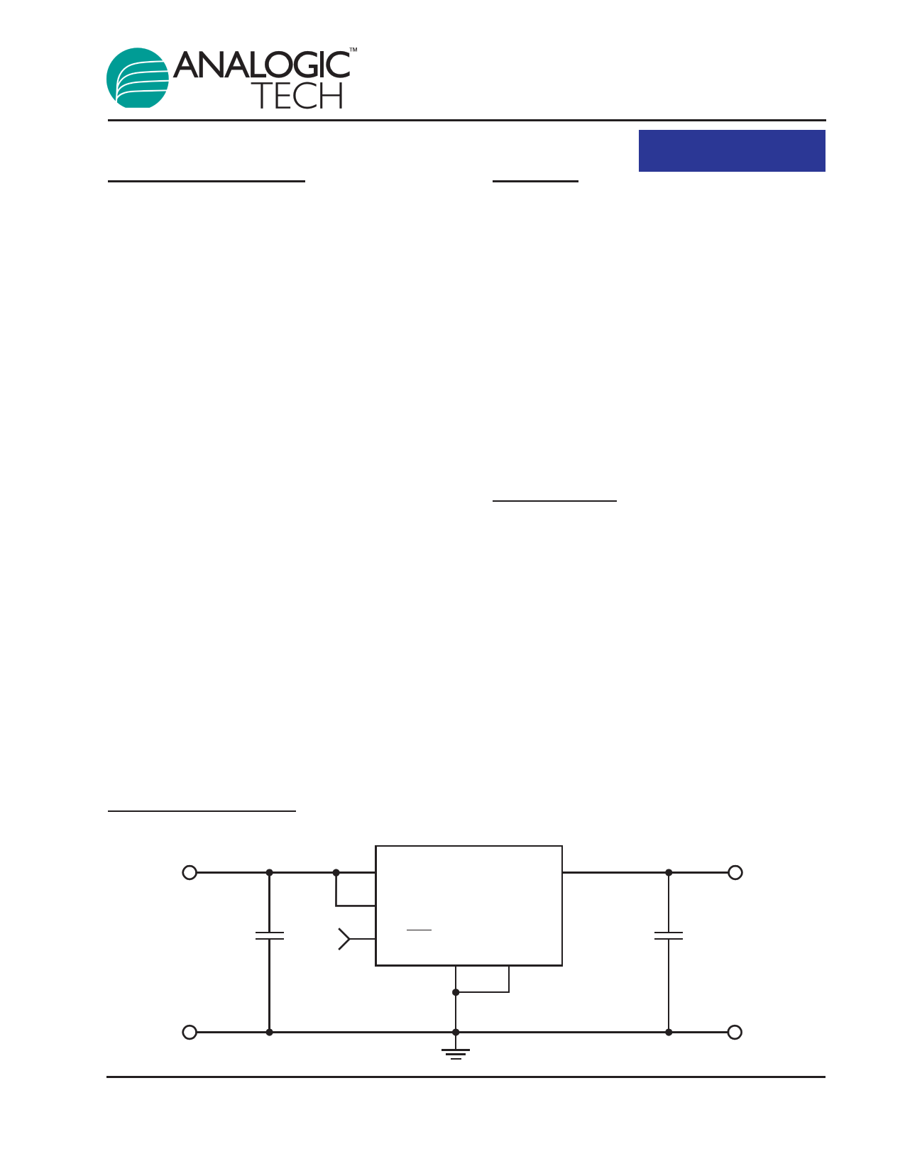
Typical Application
V IN
C IN
1µF
IN OUT
IN AAT4280A
ON ON/OFF
GND GND
GND
4280A.2005.11.1.3
V OUT
C OUT
0.1µF
GND
1
1 page 
AAT4280A
Slew Rate Controlled Load Switch
Typical Characteristics
Unless otherwise noted, VIN = 5V, TA = 25°C.
Quiescent Current vs. Temperature
50
40
30
20
10
0
-40
-20
0 20 40 60
Temperature (°C)
80 100
RDS(ON) vs. Input Voltage
270
250
230 2A
210
190 1A
170 500mA
150
130
110
90 100mA
70
1.5 1.8 2.0 2.3 2.5 2.8 3.0 3.3 3.5 3.8 4.0 4.3 4.5 4.8 5.0 5.3 5.5
Input Voltage (V)
RDS(ON) vs. Temperature
120
110
100
90
80
70
60
50
40
-40
-20
VIN = 3V
VIN = 5V
0 20 40 60
Temperature (°C)
80 100
Off-Switch Current vs. Temperature
1.000
0.100
0.010
0.001
-40
-20
0 20 40 60
Temperature (°C)
80 100
4280A.2005.11.1.3
ON/OFF Threshold vs. Input Voltage
2.2
2.0
1.8
1.6
1.4
1.2 VIH
1.0
0.8 VIL
0.6
0.4
1.4 1.9 2.4 2.9 3.4 3.9 4.4 4
Input Voltage (V)
5.4
5
5 Page 
AAT4280A
Slew Rate Controlled Load Switch
sipation and the RDS of the MOSFET at TJ(MAX).
The maximum RDS of the MOSFET at TJ(MAX) is cal-
culated by increasing the maximum room tempera-
ture RDS by the RDS temperature coefficient. The
temperature coefficient (TC) is 2800ppm/°C.
Therefore,
MAX RDS125°C = RDS25°C × (1 + TC × ∆T)
MAX RDS125°C = 120mΩ × (1 + 0.0028 ×
(125°C - 25°C)) = 154mΩ
For maximum current, refer to the following equation:
IOUT(MAX) <
PD(MAX)
RDS
For example, if VIN = 5V, RDS(MAX) = 154mΩ and TA
= 25°C, IOUT(MAX) = 2.3A. If the output load current
were to exceed 2.3A or if the ambient temperature
were to increase, the internal die temperature
would increase and the device would be damaged.
Higher peak currents can be obtained with the
AAT4280A. To accomplish this, the device thermal
resistance must be reduced by increasing the heat
sink area or by operating the load switch in a duty-
cycle manner.
High Peak Output Current Applications
Some applications require the load switch to oper-
ate at a continuous nominal current level with short
duration, high-current peaks. The duty cycle for
both output current levels must be taken into
account. To do so, first calculate the power dissi-
pation at the nominal continuous current level, and
then add in the additional power dissipation due to
the short duration, high-current peak scaled by the
duty factor.
For example, a 4V system using an AAT4280A
operates at a continuous 100mA load current level
and has short 2A current peaks, as in a GSM appli-
cation. The current peak occurs for 576µs out of a
4.61ms period.
First, the current duty cycle is calculated:
% Peak Duty Cycle: X/100 = 576µs/4.61ms
% Peak Duty Cycle = 12.5%
The load current is 100mA for 87.5% of the 4.61ms
period and 2A for 12.5% of the period. Since the
Electrical Characteristics do not report RDS(MAX) for
4V operation, it must be calculated approximately
by consulting the chart of RDS(ON) vs. VIN. The RDS
reported for 5V can be scaled by the ratio seen in
the chart to derive the RDS for a 4V VIN: 120mΩ ×
87mΩ /80mΩ = 130mΩ. De-rated for temperature:
130mΩ x (1 + 0.0028 × (125°C -25°C)) = 166mΩ.
The power dissipation for a 100mA load is calculat-
ed as follows:
PD(MAX) = IOUT2 × RDS
PD(100mA) = (100mA)2 × 166mΩ
PD(100mA) = 1.66mW
PD(87.5%D/C) = %DC × PD(100mA)
PD(87.5%D/C) = 0.875 × 1.66mW
PD(87.5%D/C) = 1.45mW
The power dissipation for 100mA load at 87.5%
duty cycle is 1.45mW. Now the power dissipation
for the remaining 12.5% of the duty cycle at 2A is
calculated:
PD(MAX) = IOUT2 × RDS
PD(2A) = (2A)2 × 166mΩ
PD(2A) = 664mW
PD(12.5%D/C) = %DC × PD(2A)
PD(12.5%D/C) = 0.125 × 664mW
PD(12.5%D/C) = 83mW
The power dissipation for 2A load at 12.5% duty
cycle is 83mW. Finally, the two power figures are
summed to determine the total true power dissipa-
tion under the varied load:
PD(total) = PD(100mA) + PD(2A)
PD(total) = 1.45mW + 83mW
PD(total) = 84.5mW
The maximum power dissipation for the AAT4280A
operating at an ambient temperature of 85°C is
333mW. The device in this example will have a
total power dissipation of 84.5mW. This is well
within the thermal limits for safe operation of the
device; in fact, at 85°C, the AAT4280A will handle
a 2A pulse for up to 50% duty cycle. At lower ambi-
ent temperatures, the duty cycle can be further
increased.
4280A.2005.11.1.3
11
11 Page | ||
| Páginas | Total 14 Páginas | |
| PDF Descargar | [ Datasheet AAT4280A.PDF ] | |
Hoja de datos destacado
| Número de pieza | Descripción | Fabricantes |
| AAT4280 | Slew Rate Controlled Load Switch | Advanced Analogic Technologies |
| AAT4280-1 | Slew Rate Controlled Load Switch | Advanced Analogic Technologies |
| AAT4280-2 | Slew Rate Controlled Load Switch | Advanced Analogic Technologies |
| AAT4280-3 | Slew Rate Controlled Load Switch | Advanced Analogic Technologies |
| Número de pieza | Descripción | Fabricantes |
| SLA6805M | High Voltage 3 phase Motor Driver IC. |
Sanken |
| SDC1742 | 12- and 14-Bit Hybrid Synchro / Resolver-to-Digital Converters. |
Analog Devices |
|
DataSheet.es es una pagina web que funciona como un repositorio de manuales o hoja de datos de muchos de los productos más populares, |
| DataSheet.es | 2020 | Privacy Policy | Contacto | Buscar |