|
|
|
PDF STP130NH02L Data sheet ( Hoja de datos )
| Número de pieza | STP130NH02L | |
| Descripción | N-channel Power MOSFET | |
| Fabricantes | ST Microelectronics | |
| Logotipo | ||
Hay una vista previa y un enlace de descarga de STP130NH02L (archivo pdf) en la parte inferior de esta página. Total 13 Páginas | ||
|
No Preview Available !
www.DataSheet4U.com
STB130NH02L
STP130NH02L
N-CHANNEL 24V - 0.0034 Ω - 120A D²PAK/TO-220
STripFET™ III POWER MOSFET FOR DC-DC CONVERSION
Table 1: General Features
TYPE
VDSS
RDS(on)
ID
STB130NH02L
STP130NH02L
24 V
24 V
< 0.0044 Ω 90 A(2)
< 0.0044 Ω 90 A(2)
■ TYPICAL RDS(on) = 0.0034 Ω @ 10 V
■ TYPICAL RDS(on) = 0.005 Ω @ 5 V
■ RDS(ON) * Qg INDUSTRY’s BENCHMARK
■ CONDUCTION LOSSES REDUCED
■ SWITCHING LOSSES REDUCED
■ LOW THRESHOLD DEVICE
■ SURFACE-MOUNTING D2PAK (TO-263)
POWER PACKAGE IN TUBE (NO SUFFIX) OR
IN TAPE & REEL (SUFFIX “T4”)
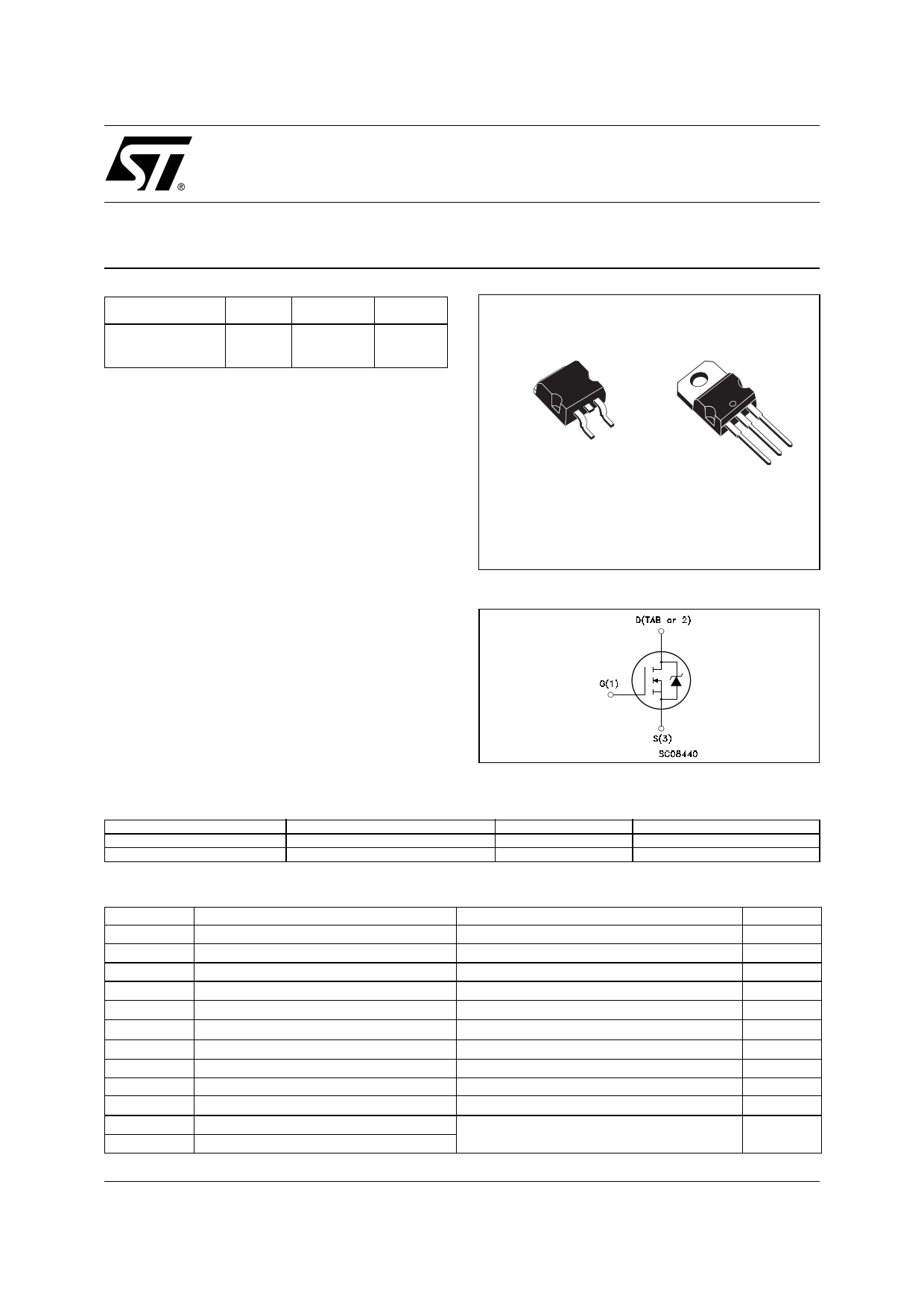
Figure 1:Package
3
1
D2PAK
TO-263
(Suffix “T4”)
3
2
1
TO-220
DESCRIPTION
The STB_P130NH02L utilizes the latest advanced
design rules of ST’s proprietary STripFET™ technology.
It is ideal in high performance DC-DC converter
applications where efficiency is to be achieved at very
high output currents.
APPLICATIONS
■ SYNCHRONOUS RECTIFICATIONS FOR
TELECOM AND COMPUTER
■ OR-ING DIODE
Figure 2: Internal Schematic Diagram
Table 2: Ordering Information
SALES TYPE
STB130NH02LT4
STP130NH02L
MARKING
B130NH02L
P130NH02L
ABSOLUTE MAXIMUM RATINGS
Symbol
Parameter
Vspike(1)
VDS
VDGR
Drain-source Voltage Rating
Drain-source Voltage (VGS = 0)
Drain-gate Voltage (RGS = 20 kΩ)
VGS Gate- source Voltage
ID(2) Drain Current (continuous) at TC = 25°C
ID(2)
IDM(3)
Drain Current (continuous) at TC = 100°C
Drain Current (pulsed)
Ptot Total Dissipation at TC = 25°C
Derating Factor
EAS (4) Single Pulse Avalanche Energy
Tstg Storage Temperature
Tj Max. Operating Junction Temperature
April 2005
PACKAGE
TO-263
TO-220
PACKAGING
TAPE & REEL
TUBE
Value
30
24
24
± 20
90
90
360
150
1
900
-55 to 175
Rev. 2.0
Unit
V
V
V
V
A
A
A
W
W/°C
mJ
°C
1/13
1 page 
Figure 11: Normalized Gate Threshold Voltage vs
Temperature
STB130NH02L STP130NH02L
Figure 12: Normalized on Resistance vs Temperature
Figure 13: Source-drain Diode Forward Characteristics
Figure 14: Normalized Breakdown Voltage vs
Temperature
..
5/13
5 Page 
STB130NH02L STP130NH02L
Pconduction
Pswitching
High Side Switch (SW1)
R DS(on)SW1 * I2L * δ
Low Side Switch (SW2)
R DS(on)SW2 * I2L * (1 − δ )
Vin
* (Q gsth(SW1)
+ Q gd(SW1)
)*f
*
IL
Ig
Zero Voltage Switching
Pdiode Recovery
Conduction
Pgate(Q G )
PQoss
Not Applicable
Not Applicable
Qg(SW1) * Vgg * f
Vin * Qoss(SW1) * f
2
1 Vin * Qrr(SW2) * f
Vf(SW2) * I L * t deadtime * f
Q gls(SW2) * Vgg * f
Vin * Qoss(SW2) * f
2
Parameter
d
Qgsth
Qgls
Pconduction
Pswitching
Pdiode
Pgate
PQoss
Meaning
Duty-cycle
Post threshold gate charge
Third quadrant gate charge
On state losses
On-off transition losses
Conduction and reverse recovery diode losses
Gate drive losses
Output capacitance losses
1 Dissipated by SW1 during turn-on
11/13
11 Page | ||
| Páginas | Total 13 Páginas | |
| PDF Descargar | [ Datasheet STP130NH02L.PDF ] | |
Hoja de datos destacado
| Número de pieza | Descripción | Fabricantes |
| STP130NH02L | N-channel Power MOSFET | ST Microelectronics |
| Número de pieza | Descripción | Fabricantes |
| SLA6805M | High Voltage 3 phase Motor Driver IC. |
Sanken |
| SDC1742 | 12- and 14-Bit Hybrid Synchro / Resolver-to-Digital Converters. |
Analog Devices |
|
DataSheet.es es una pagina web que funciona como un repositorio de manuales o hoja de datos de muchos de los productos más populares, |
| DataSheet.es | 2020 | Privacy Policy | Contacto | Buscar |