|
|
|
PDF GF9331 Data sheet ( Hoja de datos )
| Número de pieza | GF9331 | |
| Descripción | DTV/SDTV Motion Co-processor | |
| Fabricantes | Gennum | |
| Logotipo | ||
Hay una vista previa y un enlace de descarga de GF9331 (archivo pdf) en la parte inferior de esta página. Total 30 Páginas | ||
|
No Preview Available !
www.DataSheet4U.com
Features
• support for 10/8-bit HDTV/SDTV input video signals
• seamless interface to Gennum's GF9330 high
performance de-interlacer through a filter control bus
• multi-directional edge detection and control
• support for multiplexed and non-multiplexed Y/C video
• 3-field vertical motion detection and control
• fully configurable to support custom video modes
• ability to extract HVF information from embedded TRS
• seamless interface to popular ADCs and NTSC/PAL
decoders
• user configuration through a dedicated host interface,
supporting parallel and serial interfaces
• 5V tolerant inputs
• 3.3V supply for device I/O and 2.5V for core logic
Applications
• HDTV Up/Down Converters
• Production Equipment
• Video Walls
• Projection Systems
• Plasma Displays
• LCD TVs
• Home Theatre Systems
• HD DVD Players
GF9331 HDTV/SDTV
Motion Co-processor
GF9331 Data Sheet
Device Overview
The GF9331 is a high performance motion
co-processor that is used in conjunction with Gennum's
GF9330 HDTV/SDTV 10-bit De-interlacer. Together,
the GF9331 and the GF9330 provide 10-bit broadcast
quality de-interlacing for standard and high-definition
video signals up to 1080p60.
Although the GF9330 can fully function as a stand alone
de-interlacer, the GF9331 provides added features in
the form of a filter selection control bus that enables
multi-directional edge and adaptive 3-field vertical
motion detection. Edge detection and interpolation
removes the edge artifacts that tend to occur while
de-interlacing on shallow horizontal edges while vertical
motion detection reduces motion artifacts.
Filter selection controls are sent to the GF9330 on a
pixel-by-pixel basis. The GF9331 integrates all the
necessary line delays for the motion and edge
detectors. The GF9331 also provides seamless
interfaces to off-chip SDRAMs that form the required
field delays.
Ordering Information
Part Number
GF9331-CBP
Package
328 PIN BGA
Temp. Range
0oC to 70oC
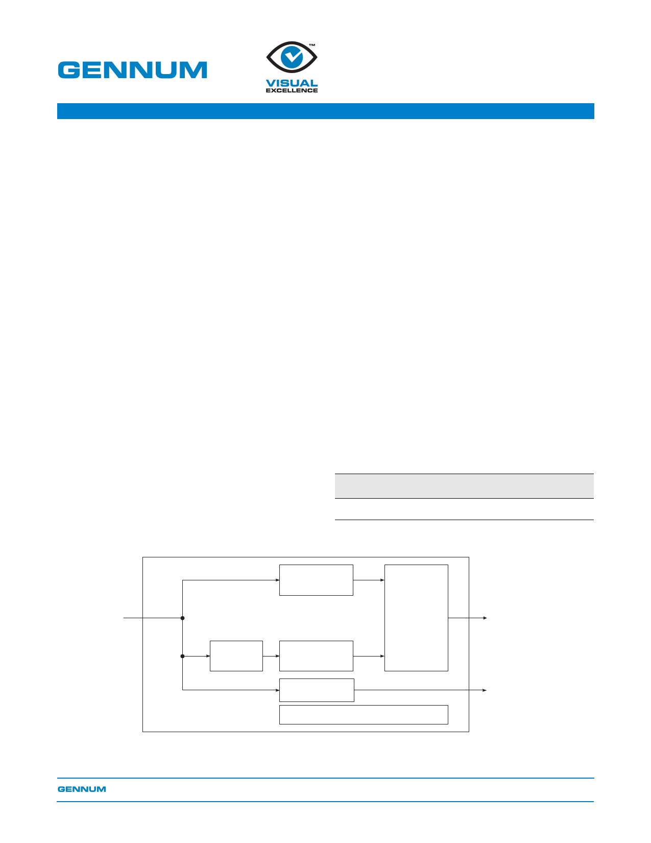
Edge Detection
Y/C
Encoder
Control bus
to GF9330
Pre-filter
Vertical Motion
Detection
Delay
External Memory Interface
Y/C Delayed Video
to GF9330
Block Diagram
Proprietary and Confidential 18303 - 4 June 2004
1 of 31
www.gennum.com
1 page 
GF9331 Data Sheet
Table 1-1: Pin Descriptions (Continued)
Symbol
R_W
A_D
Y_OUT[9:0]
C_OUT[9:0]
FIL_SEL[3:0]
H_OUT
F_OUT
V_OUT
S1_CLK
S1_CS
S1_RAS
S1_CAS
S1_WE
S1_ADDR[13:0]
S1_DAT[15:0]
S2_CLK
S2_CS
S2_RAS
S2_CAS
S2_WE
S2_ADDR[13:0]
S2_DAT[15:0]
TDI
TMS
Pin Grid
P3
P1
A20, B20, C20, C19, D20,
D19, D18, E20, E19, E18
H20, J20, J19, J18, K20,
K19, K18, L18, L19, L20
M19, M20, N19, N20
P20
T20
R20
Y10
Y5
W4
W5
Y4
Y6, W6, V6, Y7, W7, V7,
Y8, W8, V8, Y9, W9, V9,
W10, V10
V11, W11, Y11, V12, W12,
Y12, V13, W13, Y13, V14,
W14, Y14, V15, W15, Y15,
Y16
A9
A14
B15
B14
A15
A13, B13, C13, A12, B12,
C12, A11, B11, C11, C10,
B10, A10, C9, B9
C8, B8, A8, C7, B7, A7,
C6, B6, A6, C5, B5, A5,
B4, A4, B3, A3
U3
U2
Type
Description
I Host interface Read/Write control for parallel mode. A read cycle is defined
when HIGH, a write cycle is defined when LOW.
I Host interface Address/Data control for parallel mode. The data bus contains
an address when HIGH, a data word when LOW. In serial mode, this pin
serves as the chip select (active low).
O Output data bus for separate luminance or multiplexed luminance and colour
difference video data.
O Output data bus for colour difference video data.
O Filter selection control bus output to the GF9330. The FIL_SEL[3:0] bus is
used to switch the GF9330’s internal directional filters on a pixel by pixel basis.
O Output control signal. H_OUT is a horizontal blanking output.
O Output control signal. F_OUT is an ODD/EVEN field indicator.
O Output control signal. V_OUT is a vertical blanking output.
O SDRAM bank 1 clock.
O Active low SDRAM chip select for Field Buffer 1.
O Active low SDRAM row address strobe for Field Buffer 1.
O Active low SDRAM column address strobe for Field Buffer 1.
O Active low SDRAM write enable for Field Buffer 1.
O SDRAM address for Field Buffer 1.
I/O SDRAM data for Field Buffer 1.
O SDRAM bank 2 clock.
O Active low SDRAM chip select for Field Buffer 2.
O Active low SDRAM row address strobe for Field Buffer 2.
O Active low SDRAM column address strobe for Field Buffer 2.
O Active low SDRAM write enable for Field Buffer 2.
O SDRAM address for Field Buffer 2.
I/O SDRAM data for Field Buffer 2.
I JTAG data input; connect to GND if not used.
I JTAG mode select; connect to GND if not used.
Proprietary and Confidential 18303 - 4 June 2004
5 of 31
5 Page 
GF9331 Data Sheet
Table 3-1: Encoding of STD[4:0] for Selecting Input Data Format (Continued)
STD
13
14
15
16
17
18
19
20
21
22
23
24
25
26
27
28
STD[4:0]
01101
01110
01111
10000
10001
10010
10011
10100
10101
10110
10111
11000
11001
11010
11011
11100
Description
625p (50Hz) 16 x 9 with 18MHz sampling. YCbCr data stream applied to Y_IN. C_IN should be set LOW.
Timing information is extracted from embedded TRS sequences.
NOTE: Input clock is 72MHz.
Generic SD input data format with 4:1:1 sampling. YCbCr data is applied to both Y_IN and C_IN. The
externally supplied F, V and H signals are used to synchronize the input data stream.
NOTE: Input clock is 27MHz.
Generic SD input data format with 4:2:2 sampling and single multiplexed YCbCr input format. YCbCr data
applied to Y_IN. C_IN should be set LOW. The externally supplied F, V and H signals are used to synchronize
the input data stream.
NOTE: Input clock is 27 or 36MHz.
720p (60 & 60/1.001Hz) SMPTE 296M-2001. Y Data applied to Y_IN. Cb Cr data applied to C_IN.
NOTE: Input clock is 74.25MHz or 74.25/1.001MHz.
720p (30 & 30/1.001Hz) SMPTE 296M-2001. Y Data applied to Y_IN. Cb Cr data applied to C_IN.
NOTE: Input clock is 74.25MHz or 74.25/1.001MHz.
1080p (30 & 30/1.001Hz) SMPTE 274M. Y data applied to Y_IN. Cb Cr data applied to C_IN.
NOTE: Input clock is 74.25MHz or 74.25/1.001MHz.
720p (50Hz) SMPTE 296M-2001. Y Data applied to Y_IN. Cb Cr data applied to C_IN.
NOTE: Input clock is 74.25MHz.
1080p (25Hz) SMPTE 274M. Y data applied to Y_IN. Cb Cr data applied to C_IN.
NOTE: Input clock is 74.25MHz.
720p (25Hz) SMPTE 296M-2001. Y Data applied to Y_IN. Cb Cr data applied to C_IN.
NOTE: Input clock is 74.25MHz.
1080p (24 & 24/1.001Hz) SMPTE 274M. Y data applied to Y_IN. Cb Cr data applied to C_IN.
NOTE: Input clock is 74.25MHz or 74.25/1.001MHz.
720p (24 & 24/1.001Hz) SMPTE 296M-2001. Y Data applied to Y_IN. Cb Cr data applied to C_IN.
NOTE: Input clock is 74.25MHz or 74.25/1.001MHz.
1080i (30 & 30/1.001Hz) SMPTE 274M. Y data applied to Y_IN. Cb/Cr data applied to C_IN.
NOTE: Input clock is 74.25 MHz or 74.25/1.001MHz.
1080p (30 & 30/1.001Hz in Segmented Frame Format) SMPTE RP211-2000. Y data applied to Y_IN. Cb Cr
data applied to C_IN.
NOTE: Input clock is 74.25MHz or 74.25/1.001MHz.
1080i (25Hz) SMPTE 274. Y data applied to Y_IN. Cb Cr data applied to C_IN.
NOTE: Input clock is 74.25MHz.
1080p (25Hz in Segmented Frame Format) SMPTE RP211-2000. Y data applied to Y_IN. Cb Cr data applied
to C_IN.
NOTE: Input clock is 74.25MHz.
1080i (25Hz) SMPTE 295M. Y data applied to Y_IN. Cb Cr data applied to C_IN.
NOTE: Input clock is 74.25MHz.
Proprietary and Confidential 18303 - 4 June 2004
11 of 31
11 Page | ||
| Páginas | Total 30 Páginas | |
| PDF Descargar | [ Datasheet GF9331.PDF ] | |
Hoja de datos destacado
| Número de pieza | Descripción | Fabricantes |
| GF9330 | High Performance HDTV/SDTV Deinterlacer | Gennum |
| GF9331 | DTV/SDTV Motion Co-processor | Gennum |
| Número de pieza | Descripción | Fabricantes |
| SLA6805M | High Voltage 3 phase Motor Driver IC. |
Sanken |
| SDC1742 | 12- and 14-Bit Hybrid Synchro / Resolver-to-Digital Converters. |
Analog Devices |
|
DataSheet.es es una pagina web que funciona como un repositorio de manuales o hoja de datos de muchos de los productos más populares, |
| DataSheet.es | 2020 | Privacy Policy | Contacto | Buscar |