|
|
|
PDF VMX51C900 Data sheet ( Hoja de datos )
| Número de pieza | VMX51C900 | |
| Descripción | Versa Mix 8051 MCU | |
| Fabricantes | Ramtron | |
| Logotipo | ||
Hay una vista previa y un enlace de descarga de VMX51C900 (archivo pdf) en la parte inferior de esta página. Total 30 Páginas | ||
|
No Preview Available !
www.DataSheet4U.com
VMX51C900
Datasheet
Rev 1.2
Versa Mix 8051 MCU with LCD Controller and ADC
Overview
The VMX51C900 is an 8-bit microcontroller with 8KB of
Flash memory, 256 bytes of RAM and based on the
architecture of the standard 80C51 microcontroller.
The VMX51C900 includes extra features such as a 4
Channel 8-bit A/D Converter, 2 PWM outputs and 14
segment x 4 common LCD driver. The VMX51C900
hardware features make it a versatile and cost-effective
controller for a wide range of embedded applications.
The Flash memory can be programmed using a parallel
programmer available from Ramtron. Support is also
available from 3rd party commercial programmer
manufacturers.
The VMX51C900 is available in PLCC-44, QFP-44 and
DIP-40 packages and operates over the industrial
temperature range.
Features
• 80C51/80C52 pin compatible
• 8KB on-chip Flash memory
• 256 Bytes on-chip data RAM
• 4 8-bit I/O ports and 1 4-bit I/O port
• 4-Channel, 8-bit A/D Converter
• LCD Driver: 14-Segment x 4-Common
• 2-PWM Outputs
• UART serial port
• 3 16-bit Timers/Counters
• Watchdog Timer
• BCD arithmetic + 8-bit Unsigned Multiply and Division
• 2 levels of Interrupt Priority and nested Interrupts
• Power saving modes
• Low EMI (ALE disable)
• Code protection function
• Operates at a clock frequency of up to 25MHz
• Industrial Temperature range (-40°C to +85°C)
• 5V version available
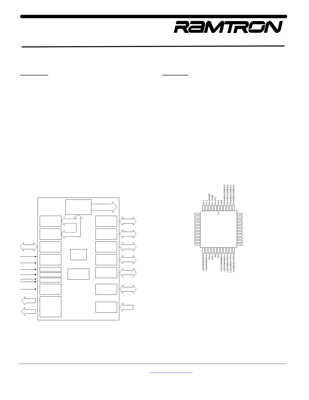
FIGURE 2: VMX51C900 PLCC-44 AND QFP-44 PIN OUT DIAGRAMS
FIGURE 1: VMX51C900 BLOCK DIAGRAM
8KB
FLASH
256 Bytes of
RAM
UART
Serial port
2 INTERRUPT
INPUTS
TIMER 0
TIMER 1
TIMER 2
RESET
8051
PROCESSOR
ADDRESS/
DATA BUS
PORT 0
PORT 1
POWER
CONTROL
PORT 2
PORT 3
WATCHDOG
TIMER
PORT 4
PWM
14 segments
4 Commons
LCD Driver
8 bit A/D
Converter
(4 Inputs)
8
8
8
8
4
2
4 Channel
PWMB/P1.5
P1.6
P1.7
RES
RXD/P3.0
P4.3
TXD/P3.1
#INT0/P3.2
#INT1/P3.3
ADCIN0/T0/P3.4
ADCIN1/T1/P3.5
6
7
17
18
40
39
VMX51C900
PLCC-44
29
28
P0.4/AD4/LCDSEG9
P0.5/AD5/LCDSEG8
P0.6/AD6/LCDSEG7
P0.7/AD7/LCDSEG6
#EA
P4.1
ALE/LCDSEG5
#PSEN/LCDSEG4
P2.7/A15/LCDSEG3
P2.6/A14/LCDSEG2
P2.5/A13/LCDSEG1
Ramtron International Corporation ? http://www.ramtron.com
1850 Ramtron Drive Colorado Springs ? MCU customer service: 1-800-943-4625, 1-514-871-2447, ext. 208
Colorado, USA, 80921 ? 1-800-545-FRAM, 1-719-481-7000
page 1 of 55
1 page 
VMX51C900
DIP-40 Pin Descriptions
TABLE 3: VMX51C900 PIN DESCRIPTIONS FOR DIP40 PACKAGE
DIP -
40
1
2
3
4
5
6
7
8
9
10
11
12
13
14
15
16
17
18
19
20
21
22
23
24
25
26
27
Name
T2
P1.0
T2EX
P1.1
P1.2
PWMA
P1.3
P1.4
PWMB
P1.5
P1.6
P1.7
RES
RXD
P3.0
TXD
P3.1
#INT0
P3.2
#INT1
P3.3
ADCIN0
T0
P3.4
ADCIN1
T1
P3.5
ADCIN2
#WR
P3.6
ADCIN3
#RD
P3.7
XTAL2
XTAL1
VSS
LCDCOM0
P2.0
A8
LCDCOM1
P2.1
A9
LCDCOM2
P2.2
A10
LCDCOM3
P2.3
A11
LCDSEG0
P2.4
A12
LCDSEG1
P2.5
A13
LCDSEG2
P2.6
A14
I/O Function
I Timer 2 Clock Out
I/O Bit 0 of Port 1
I Timer 2 Control
I/O Bit 1 of Port 1
I/O Bit 2 of Port 1
O PWM Channel A
I/O Bit 3 of Port 1
I/O Bit 4 of Port 1
O PWM Channel B
I/O Bit 5 of Port 1
I/O Bit 6 of Port 1
I/O Bit 7 of Port 1
I Reset
I Receive Data
I/O Bit 0 of Port 3
O Transmit Data &
I/O Bit 1 of Port 3
I External Interrupt 0
I/O Bit 2 of Port 3
I External Interrupt 1
I/O Bit 3 of Port 3
Ain ADC input 0
I Timer 0
I/O Bit 4 of Port 3
Ain ADC input 1
I Timer 1 & 3
I/O Bit 5 of Port
Ain ADC input 2
O Ext. Memory Write
I/O Bit 6 of Port 3
Ain ADC input 3
O Ext. Memory Read
I/O Bit 7 of Port 3
O Oscillator/Crystal Output
I Oscillator/Crystal In
- Ground
- LCD Driver Common 0
I/O Bit 0 of Port 2
O Bit 8 of Ext. Memory Address
- LCD Driver Common 1
I/O Bit 1 of Port 2
O Bit 9 of Ext. Memory Address
- LCD Driver Common 2
I/O Bit 2 of Port 2
O Bit 10 of Ext. Memory Address
- LCD Driver Common 3
I/O Bit 3 of Port 2 &
O Bit 11 of Ext. Memory Address
- LCD Segment 0
I/O Bit 4 of Port 2
O Bit 12 of Ext. Memory Address
- LCD Segment 1
I/O Bit 5 of Port 2
O Bit 13 of External Memory Address
- LCD Segment 2
I/O Bit 6 of Port 2
O Bit 14 of External Memory Address
PLCC
- 44
Name
I/O
Function
LCDSEG3 -
LCD Segment 3
28 P2.7
I/O Bit 7 of Port 2
A15 O Bit 15 of External Memory Address
29
LCDSEG4
#PSEN
-
O
LCD Segment 4
Program Store Enable
30
LCDSEG5
ALE
-
O
LCD Segment 5
Address Latch Enable
31 #EA
I External Access
LCDSEG6 -
LCD Segment 6
32 P0.7
I/O Bit 7 Of Port 0
AD7
I/O Data/Address Bit 7 of Ext. Memory
LCDSEG7 -
LCD Segment 7
33 P0.6
I/O Bit 6 of Port 0
AD6
I/O Data/Address Bit 6 of Ext. Memory
LCDSEG8 -
LCD Segment 8
34 P0.5
I/O Bit 5 of Port 0
AD5
I/O Data/Address Bit 5 of Ext. Memory
LCDSEG9 -
LCD Segment 9
35 P0.4
I/O Bit 4 of Port 0
AD4
I/O Data/Address Bit 4 of Ext. Memory
LCDSEG10 -
LCD Segment 10
36 P0.3
I/O Bit 3 Of Port 0
AD3
I/O Data/Address Bit 3 of Ext. Memory
LCDSEG11 -
LCD Segment 11
37 P0.2
I/O Bit 2 of Port 0
AD2
I/O Data/Address Bit 2 of Ext. Memory
LCDSEG12 -
LCD Segment 12
38 P0. 1
I/O Bit 1 of Port 0 & Data
AD1
I/O Address Bit 1 of Ext. Memory
LCDSEG13 -
LCD Segment 13
39 P0.0
I/O Bit 0 Of Port 0 & Data
AD0
I/O Address Bit 0 of Ext. Memory
40 VDD
- 5V supply
T2 / P1.0
T2EX / P1.1
PWMA / P1.2
P1.3
P1.4
PWMB / P1.5
P1.6
P1.7
RESET
RXD / P3.0
TXD / P3.1
#INT0 / P3.2
#INT1 / P3.3
ADCIN0 / T0 / P3.4
ADCIN1 / T1 / P3.5
ADCIN2 / #WR / P3.6
ADCIN3 / #RD / P3.7
XTAL2
XTAL1
VSS
1
2
3
4
5
6
7
8
9
VMX51C900
10 DIP-40
11
12
13
14
15
16
17
18
19
20
40
39
38
37
36
35
34
33
32
31
30
29
28
27
26
25
24
23
22
21
VDD
P0.0 / AD0 / LCDSEG13
P0.1 / AD1 / LCDSEG12
P0.2 / AD2 / LCDSEG11
P0.3 / AD3 / LCDSEG10
P0.4 / AD4 / LCDSEG9
P0.5 / AD5 / LCDSEG8
P0.6 / AD6 / LCDSEG7
P0.7 / AD7 / LCDSEG6
#EA / VPP
ALE / LCDSEG5
PSEN / LCDSEG4
P2.7 / A15 / LCDSEG3
P2.6 / A14 / LCDSEG2
P2.5 / A13 / LCDSEG1
P2.4 / A12 / LCDSEG0
P2.3 / A11 / LCDCOM3
P2.2 / A10 / LCDCOM2
P2.1 / A9 / LCDCOM1
P2.0 / A8 / LCDCOM0
_______________________________________________________________________________________________
www.ramtron.com
page 5 of 55
5 Page 
VMX51C900
VMX51C900 EA pin is held at 0V during reset, or
when a MOVX instruction is executed.
The P0 register located at address 80h controls the
individual pin direction when configured as an I/O. The
P0 register is bit-addressable.
TABLE 10: PORT 0 REGISTER (P0) - SFR 80H
76543210
P0.7 P0.6 P0.5 P0.4 P0.3 P0.2 P0.1 P0.0
Bit Mnemonic Description
7 P0.7
For each bit of the P0 register correspond
6 P0.6
to an I/O line:
5 P0.5
4 P0.4
3 P0.3
2 P0.2
0: Output transistor pull the line to 0V
1: The output transistor is blocked so the
pull-up brings the I/O to 5V.
1 P0.1
0 P0.0
Port 2
Port P2 is very similar to Port1 and Port3, the
difference being that the alternate function of P2 is to
act as the upper address bus (A8-A15) when the EA
line of the VMX51C900 is held low at reset time or
when a MOVX instruction is executed.
Like the P1, P2 and P3 registers, the P2 register is bit-
addressable.
TABLE 11: PORT 2 REGISTER (P2) - SFR A0H
76543
P2.7 P2.6 P2.5 P2.4 P2.3
2
P2.2
1
P2.1
0
P2.0
Bit Mnemonic Description
7 P2.7
For each bit of the P2 register correspond
6 P2.6
to an I/O line:
5 P2.5
4 P2.4
3 P2.3
2 P2.2
0: Output transistor pull the line to 0V
1: The output transistor is blocked so the
pull-up brings the I/O to 5V.
1 P2.1
0 P2.0
Port P0 and P2 as Address and Data Bus
The output stage may receive data from two sources:
• The outputs of register P0 or the bus address
itself multiplexed with the data bus for P0
• The outputs of the P2 register or the high byte
(A8 through A15) of the bus address for the P2
port
FIGURE 4: P2 PORT STRUCTURE
Read Register
Address
Internal Bus
Write to
Register
Q
D Flip-Flop
Q
Control
Vcc
Pull-up
Network
X1
IC Pin
Read Pin
When the ports are used as an address or data bus,
the special function registers P0 and P2 are
disconnected from the output stage, the 8 bits of the
P0 register are forced to 1 and the contents of the P2
register remains constant.
Port 1
The P1 register controls the direction of the Port 1 I/O
pins. Writing a 1 to the corresponding bit configures
the port as an output. This presents a logic 1 to the
corresponding I/O pin or allows the I/O pin to be used
as an input. Writing a 0 activates the output “pull-
down” transistor, which will force the corresponding I/O
line to a logic low.
TABLE 12: PORT 1 REGISTER (P2) - SFR 90H
76543
P1.7 P1.6 P1.5 P1.4 P1.3
2
P1.2
1
P1.1
0
P1.0
Bit Mnemonic Description
7 P1.7
For each bit of the P1 register correspond
6 P1.6
to an I/O line:
5 P1.5
4 P1.4
3 P1.3
2 P1.2
0: Output transistor pulls the line to 0V
1: The output transistor is blocked so the
pull-up brings the I/O to 5V
1 P1.1
0 P1.0
______________________________________________________________________________________________
www.ramtron.com
page 11 of 55
11 Page | ||
| Páginas | Total 30 Páginas | |
| PDF Descargar | [ Datasheet VMX51C900.PDF ] | |
Hoja de datos destacado
| Número de pieza | Descripción | Fabricantes |
| VMX51C900 | Versa Mix 8051 MCU | Ramtron |
| Número de pieza | Descripción | Fabricantes |
| SLA6805M | High Voltage 3 phase Motor Driver IC. |
Sanken |
| SDC1742 | 12- and 14-Bit Hybrid Synchro / Resolver-to-Digital Converters. |
Analog Devices |
|
DataSheet.es es una pagina web que funciona como un repositorio de manuales o hoja de datos de muchos de los productos más populares, |
| DataSheet.es | 2020 | Privacy Policy | Contacto | Buscar |