|
|
|
PDF VIPER20A-E Data sheet ( Hoja de datos )
| Número de pieza | VIPER20A-E | |
| Descripción | SMPS primary IC | |
| Fabricantes | ST Microelectronics | |
| Logotipo | ||
Hay una vista previa y un enlace de descarga de VIPER20A-E (archivo pdf) en la parte inferior de esta página. Total 30 Páginas | ||
|
No Preview Available !
www.DataSheet4U.com
VIPer20A-E
SMPS primary I.C.
General features
Type
VIPer20A-E
VIPer20ASP-E
VIPer20ADIP-E
VDSS
700V
700V
700V
In RDS(on)
0.5A
0.5A
0.5A
18Ω
18Ω
18Ω
■ Adjustable switching frequency up to 200 kHz
■ Current mode control
■ Soft start and shutdown control
■ Automatic burst mode operation in stand-by
condition able to meet “blue angel” norm (<1w
total power consumption)
■ Internally trimmed zener reference
■ Undervoltage lock-out with hysteresis
■ Integrated start-up supply
■ Over-temperature protection
■ Low stand-by current
■ Adjustable current limitation
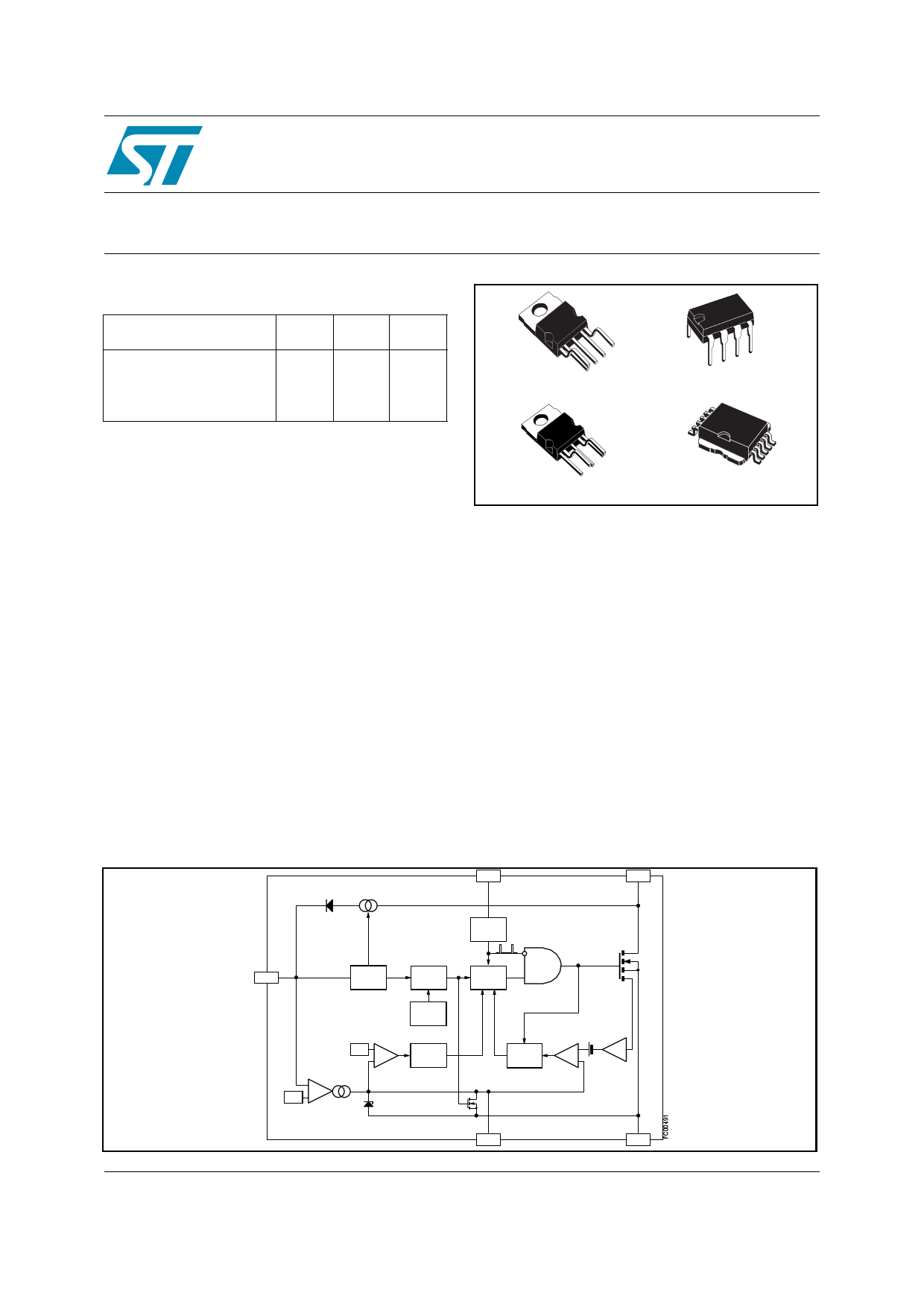
Block diagram
PENTAWATT HV
DIP-8
PENTAWATT HV (022Y)
10
1
POWERSO-10TM
Description
All the devices are made using VIPower M0
Technology, combines on the same silicon chip a
state-of-the-art PWM circuit together with an
optimized, high voltage, Vertical Power MOSFET
(700V/ 0.5A).
Typical applications cover offline power supplies
with a secondary power capability of 10W in wide
range condition and 20W in single range or with
doubler configuration. It is compatible from both
primary or secondary regulation loop despite
using around 50% less components when
compared with a discrete solution. Burst mode
operation is an additional feature of this device,
offering the ability to operate in stand-by mode
without extra components.
OSC
DRAIN
June 2006
VDD
ON/OFF
UVLO
LOGIC
SECURITY
LATCH
R/S FF Q
S
OVERTEMP.
DETECTOR
OSCILLATOR
PWM
LATCH
S
R1 FF Q
R2 R3
13 V
0.5 V
ERROR
_ AMPLIFIER
+
_
+
4.5 V
1.7
µs
delay
250 ns
Blanking
COMP
Rev 2
0.5V
++ _
6 V/A
_
CURRENT
AMPLIFIER
SOURCE
1/34
www.st.com
34
1 page 
VIPer20A-E
Electrical data
1.2 Electrical characteristics
TJ = 25°C; VDD = 13V, unless otherwise specified
Table 2. Power section
Symbol
Parameter
Test conditions
BVDS
IDSS
RDS(on)
tf
tr
Coss
Drain-Source Voltage ID = 1mA; VCOMP = 0V
Off-State Drain
Current
VCOMP = 0V; Tj = 125°C
VDS = 700V
Static Drain-Source
On Resistance
ID = 0.4A
ID = 0.4A; TJ= 100°C
Fall Time
ID = 0.2A; VIN =300V (1) Figure 7
Rise Time
ID = 0.4A; VIN = 300V (1) Figure 7
Output Capacitance VDS = 25V
Min
700
Typ
15.5
100
50
90
Max
1.0
18
32
Unit
V
mA
Ω
Ω
ns
ns
pF
(1) On Inductive Load, Clamped.
Table 3. Supply section
Symbol
Parameter
Start-Up Charging Current
IDDch
Operating Supply Current
IDD0
IDD1
IDD2
VDDoff
VDDon
VDDhyst
Operating Supply Current
Operating Supply Current
Undervoltage Shutdown
Undervoltage Reset
Hysteresis Start-up
Table 4. Oscillator section
Symbol
Parameter
FSW
Oscillator Frequency Total
Variation
VOSCIH
VOSCIL
Oscillator Peak Voltage
Oscillator Valley Voltage
Test conditions
VDD = 5V; VDS = 35V
Figure 6, Figure 11
VDD = 12V; FSW = 0kHz
Figure 6
VDD = 12V; Fsw = 100kHz
VDD = 12V; Fsw = 200kHz
Figure 6
Figure 6
Figure 6
Test conditions
RT=8.2KΩ; CT=2.4nF
VDD=9 to 15V;
with RT± 1%; CT± 5%
(see Figure )(see Figure 14)
Min Typ Max Unit
-2 mA
12 16 mA
13 mA
14 mA
7.5 8 9 V
11 12
V
2.4 3
V
Min Typ Max Unit
90 100 110 KHz
7.1 V
3.7 V
5/34
5 Page 
VIPer20A-E
5 Operation description
Operation description
5.1 Current mode topology:
The current mode control method, like the one integrated in the devices, uses two control loops
- an inner current control loop and an outer loop for voltage control. When the Power MOSFET
output transistor is on, the inductor current (primary side of the transformer) is monitored with a
SenseFET technique and converted into a voltage VS proportional to this current. When VS
reaches VCOMP (the amplified output voltage error) the power switch is switched off. Thus, the
outer voltage control loop defines the level at which the inner loop regulates peak current
through the power switch and the primary winding of the transformer.
Excellent open loop D.C. and dynamic line regulation is ensured due to the inherent input
voltage feedforward characteristic of the current mode control. This results in improved line
regulation, instantaneous correction to line changes, and better stability for the voltage
regulation loop.
Current mode topology also ensures good limitation in case there is a short circuit. During the
first phase the output current increases slowly following the dynamic of the regulation loop.
Then it reaches the maximum limitation current internally set and finally stops because the
power supply on VDD is no longer correct. For specific applications the maximum peak current
internally set can be overridden by externally limiting the voltage excursion on the COMP pin.
An integrated blanking filter inhibits the PWM comparator output for a short time after the
integrated Power MOSFET is switched on. This function prevents anomalous or premature
termination of the switching pulse in case there are current spikes caused by primary side
capacitance or secondary side rectifier reverse recovery time.
5.2 Stand-by mode
Stand-by operation in nearly open load conditions automatically leads to a burst mode
operation allowing voltage regulation on the secondary side. The transition from normal
operation to burst mode operation happens for a power PSTBY given by :
Where:
PSTBY = 12--LPI2STBYFSW
LP is the primary inductance of the transformer. FSW is the normal switching frequency.
ISTBY is the minimum controllable current, corresponding to the minimum on time that the
device is able to provide in normal operation. This current can be computed as :
ISTBY = -(--t--b----+---L--t-d-p--)---V----I--N--
tb + td is the sum of the blanking time and of the propagation time of the internal current sense
and comparator, and represents roughly the minimum on time of the device. Note: that PSTBY
may be affected by the efficiency of the converter at low load, and must include the power
drawn on the primary auxiliary voltage.
11/34
11 Page | ||
| Páginas | Total 30 Páginas | |
| PDF Descargar | [ Datasheet VIPER20A-E.PDF ] | |
Hoja de datos destacado
| Número de pieza | Descripción | Fabricantes |
| VIPER20A-E | SMPS primary IC | ST Microelectronics |
| Número de pieza | Descripción | Fabricantes |
| SLA6805M | High Voltage 3 phase Motor Driver IC. |
Sanken |
| SDC1742 | 12- and 14-Bit Hybrid Synchro / Resolver-to-Digital Converters. |
Analog Devices |
|
DataSheet.es es una pagina web que funciona como un repositorio de manuales o hoja de datos de muchos de los productos más populares, |
| DataSheet.es | 2020 | Privacy Policy | Contacto | Buscar |