|
|
|
PDF MC33110 Data sheet ( Hoja de datos )
| Número de pieza | MC33110 | |
| Descripción | LOW VOLTAGE COMPANDER | |
| Fabricantes | Motorola Semiconductors | |
| Logotipo | ||
Hay una vista previa y un enlace de descarga de MC33110 (archivo pdf) en la parte inferior de esta página. Total 13 Páginas | ||
|
No Preview Available !
Low Voltage Compander
The MC33110 contains two variable gain circuits configured for
compressing and expanding the dynamic range of an audio signal. One
circuit is configured as an expander, while the other circuit can be configured
as a compressor or expander. Each circuit has a full wave rectifier to provide
average value information to a variable gain cell located in either the input
stage or the feedback path. An internal, temperature stable bandgap
reference provides the necessary precision voltages and currents required.
The MC33110 will operate from a supply voltage of 2.1 to 7.0 V, over a
temperature range of –40 to 85°C. The device is designed to accommodate
an 80 dB dynamic range from –60 dB to 20 dB, referenced to 100 mVrms.
Applications include cordless telephone, CB, walkie–talkie, most voice
RF links, and any application where the signal–to–noise ratio can be
improved by reducing the transmitted dynamic range. Other applications
include speakerphone and voice activated intercom, dictating machine,
standard telephone, etc.
The MC33110 is packaged in a 14 pin DIP for through–the–hole
applications and an SO–14 surface mount.
• Operating Supply Voltage: 2.1 to 7.0 V
• No Precision External Components Required
• 80 dB Dynamic Range Compressed to 40 dB, Re–expandable to 80 dB
• Unity Gain Level: 100 mVrms
• Adjustable Response Time
• Ambient Operating Temperature: –40 to 85°C
• Temperature Compensated Reference
• Applications Include Cordless Phone, CB Radio, Speakerphone, etc.
Order this document by MC33110/D
MC33110
LOW VOLTAGE
COMPANDER
SEMICONDUCTOR
TECHNICAL DATA
14
1
D SUFFIX
PLASTIC PACKAGE
CASE 751A
(SO–14)
14
1
P SUFFIX
PLASTIC PACKAGE
CASE 646
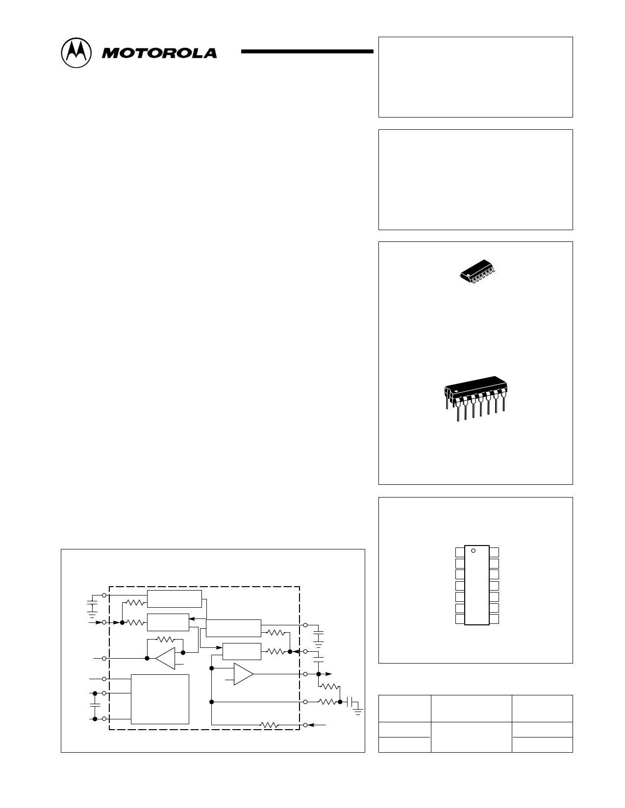
PIN CONNECTIONS
Simplified Block Diagram
2.2 µF
Exp
Input
3
5
Exp. 4
Output
14
VCC
VB
10 µF
Gnd
6
7
Rectifier
4.7 k
∆ Gain
10 k
10 k –
+
VB
Bias
&
Reference
Generator
Rectifier
∆ Gain
–
VB +
4.7 k
10 k
10 k
MOTOROLA RF/IF DEVICE DATA
12
2.2 µF
8
2.0 µF
11 Comp
Output
9 20 k 1.0 µF
20 k
10 Comp
Input
Vref 1
NC 2
Exp Filter 3
Exp Output 4
Exp Input 5
VB 6
Gnd 7
14 VCC
13 NC
12 Comp Filter
11 Comp Output
10 Comp Input
9 Inv Input
8 Comp Feedback
(Top View)
ORDERING INFORMATION
Device
Operating
Temperature Range
Package
MC33110D
MC33110P
TA = –40 to 85°C
SO–14
Plastic DIP
© Motorola, Inc. 1998
Rev 1
1
1 page 
MC33110
Compressor
Figure 2. Compressor Transfer Characteristics
1000
Expander
Figure 3. Expander Transfer Characteristics
1000
100
100
10
10
1.0
1.0
0.1
1.0 10 100
Vin, INPUT VOLTAGE (mVrms)
0.1
1000 1.0
10 100
Vin, INPUT VOLTAGE (mVrms)
1000
Figure 4. Compressor Transfer Characteristics
10
0
–10
–20
–30
–60
0 dB = 100 mVrms
–40 –20
0
Vin, INPUT VOLTAGE (dB)
+20
Figure 5. Expander Transfer Characteristics
20
0
–20
–40
–60
–30
0 dB = 100 mVrms
–20 –10
0
Vin, INPUT VOLTAGE (dB)
+10
Figure 6. Power Supply Rejection (Compressor)
40
30
CVB = 220 µF
20
CVB = 100 µF
10 CVB = 47 µF
0
CVB = 10 µF
–10
10
100
Pin 10 Input Signal = 0 mV
VCC = 5.0 V
1.0 k 10 k
f, FREQUENCY (Hz)
100 k
Figure 7. Power Supply Rejection (Expander)
50
40 CVB = 220 µF
CVB = 100 µF
30
CVB = 47 µF
20
CVB = 10 µF
10
Pin 5 Input Signal = 0 mV
VCC = 5.0 V
0
10 100 1.0 k 10 k 100 k
f, FREQUENCY (Hz)
MOTOROLA RF/IF DEVICE DATA
5
5 Page 
MC33110
APPLICATIONS INFORMATION
Signal–to–Noise Improvement
Among the basic reasons for the original development of
compander type circuits was to improve the signal–to–noise
ratio of long distance telecom circuits, and of voice circuits
which are transmitted over RF links (CBs, walkie–talkies,
cordless phones, etc.). Since much of the noise heard at the
receiving end of a transmission is due to noise picked up, for
example, in the airway portion of the RF link, the compressor
was developed to increase the low–level signals at the
transmitting end. Then any noise picked in the RF link would
be a smaller percentage of the transmitted signal level. At the
receiving end, the signal is then expanded back to its original
level, retaining the same high signal–to–noise ratio. While the
above explanation indicates it is not necessary to attenuate
strong signals (at the transmitting end), a benefit of doing this
is the reduced dynamic range which must be handled by the
system transmitter and receiver. The MC33110 was
designed for a two–to–one compression and expansion, i.e.
an 80 dB dynamic signal is compressed to a 40 dB dynamic
range, transmitted to the receiving end and then expanded
back to an 80 dB dynamic range.
The MC33110 compander is not limited to RF or long
distance telephony applications. It can be used in any system
requiring an improved signal–to–noise ratio such as
telephones, speakerphones, tape recorders, digital
recording, and many others.
Second Expander
Should the application require it, the MC33110 can be
configured as two expanders by reconfiguring the
compressor side as shown in Figure 26.
Figure 26. Second Expander
8
Input
4.7 k 12
10 k
Iref
Rectifier
IControl
10 k
∆ Gain
–
VB +
9
10
11
This circuit will provide the same performance as
the expander at Pins 3 through 5.
2.2 µF
Output
Power Supplies, Grounding
The PC board layout, the quality of the power supplies and
the ground system at the IC are very important in order to
obtain proper operation. Noise, from any source, coming into
the device on VCC or ground, can cause a distorted output, or
incorrect gain level.
VCC must be decoupled to the appropriate ground at the
IC (within 1″ max) with a 4.7 µF capacitor and a 0.01 µF
ceramic. A tantalum capacitor is recommended for the larger
value if very high frequency noise is present since electrolytic
capacitors simply have too much inductance at those
frequencies. The quality of the power supply voltage should
be checked at the IC with a high frequency scope. Noise
spikes (always present if digital circuits are near this IC) can
easily exceed 400 mV, and if they get into the IC, the output
can have noise or distortion. Noise can be reduced by
inserting resistors and/or inductors between the supply and
the IC.
If switching power supplies are used, there will usually be
spikes of 0.5 V or greater at frequencies of 50 kHz to
1.0 MHz. These spikes are generally more difficult to reduce
because of their greater energy content. In extreme cases, a
three terminal regulator (MC78L05ACP), with appropriate
high frequency filtering, should be used and dedicated to the
analog portion of the circuit.
The ripple content of the supply should not allow its
magnitude to exceed the values in the Recommended
Operating Conditions table.
The PC board tracks supplying VCC and ground to the
MC33110 should preferably not be at the tail end of the bus
distribution, after passing through a maze of digital circuitry.
The analog circuitry containing the MC33110 should be close
to the power supply, or the connector where the supply
voltages enter the board. If VCC is supplying considerable
current to other parts of the board, then it is preferable to
have dedicated lines from the supply or connector directly to
the MC33110 and associated circuitry.
PC Board Layout
Although this device is intended for use in the audio
frequency range, the amplifiers have a bandwidth of
≈300 kHz, and can therefore oscillate at frequencies outside
the voiceband should there be excessive stray capacitance
or other unintended feedback loops. A solid ground plane is
MOTOROLA RF/IF DEVICE DATA
11
11 Page | ||
| Páginas | Total 13 Páginas | |
| PDF Descargar | [ Datasheet MC33110.PDF ] | |
Hoja de datos destacado
| Número de pieza | Descripción | Fabricantes |
| MC33110 | LOW VOLTAGE COMPANDER | Motorola Semiconductors |
| MC33111 | Low Voltage Compander | Motorola Semiconductors |
| Número de pieza | Descripción | Fabricantes |
| SLA6805M | High Voltage 3 phase Motor Driver IC. |
Sanken |
| SDC1742 | 12- and 14-Bit Hybrid Synchro / Resolver-to-Digital Converters. |
Analog Devices |
|
DataSheet.es es una pagina web que funciona como un repositorio de manuales o hoja de datos de muchos de los productos más populares, |
| DataSheet.es | 2020 | Privacy Policy | Contacto | Buscar |