|
|
|
PDF MC14001B Data sheet ( Hoja de datos )
| Número de pieza | MC14001B | |
| Descripción | B-Suffix Series CMOS Gates | |
| Fabricantes | Motorola Semiconductors | |
| Logotipo | ||
Hay una vista previa y un enlace de descarga de MC14001B (archivo pdf) en la parte inferior de esta página. Total 11 Páginas | ||
|
No Preview Available !
MOTOROLA
SEMICONDUCTOR TECHNICAL DATA
B-Suffix Series CMOS Gates
The B Series logic gates are constructed with P and N channel
enhancement mode devices in a single monolithic structure (Complemen-
tary MOS). Their primary use is where low power dissipation and/or high
noise immunity is desired.
• Supply Voltage Range = 3.0 Vdc to 18 Vdc
• All Outputs Buffered
• Capable of Driving Two Low–power TTL Loads or One Low–power
Schottky TTL Load Over the Rated Temperature Range.
• Double Diode Protection on All Inputs Except: Triple Diode Protection
on MC14011B and MC14081B
• Pin–for–Pin Replacements for Corresponding CD4000 Series B Suffix
Devices (Exceptions: MC14068B and MC14078B)
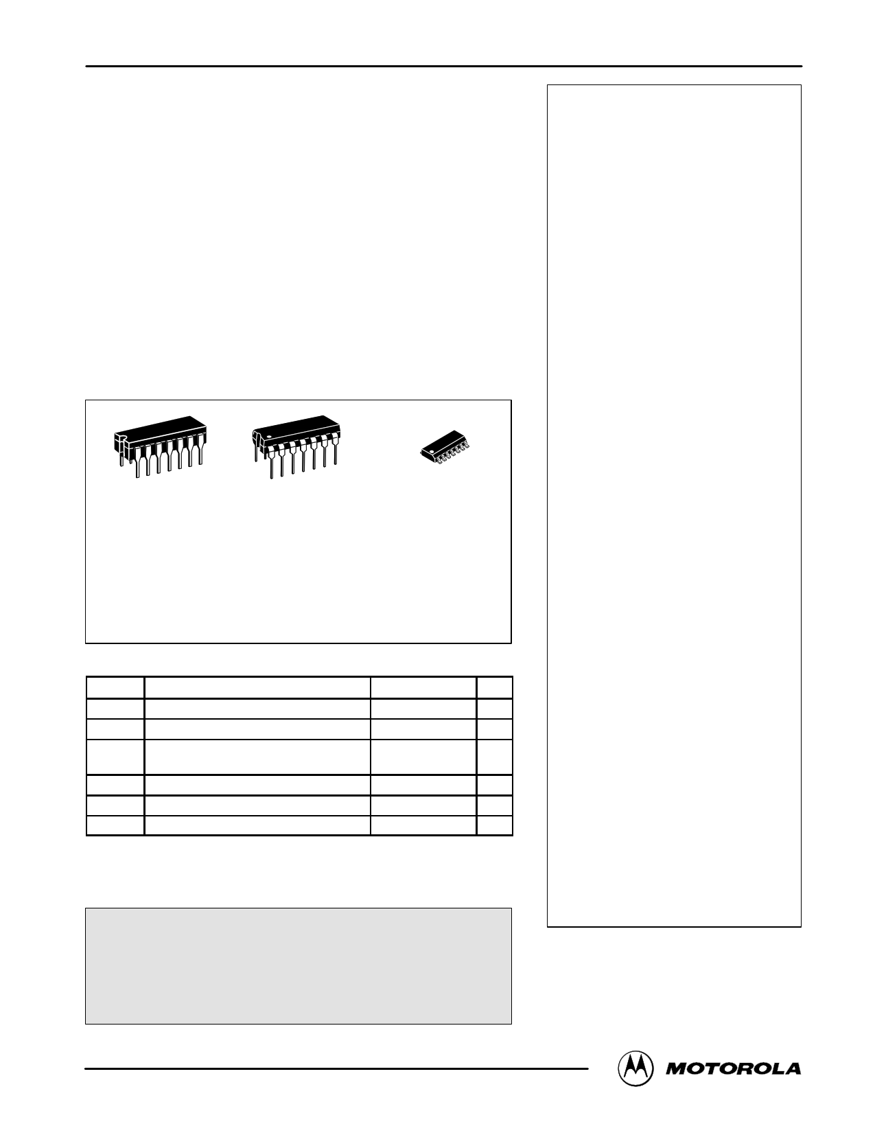
L SUFFIX
CERAMIC
CASE 632
P SUFFIX
PLASTIC
CASE 646
D SUFFIX
SOIC
CASE 751A
ORDERING INFORMATION
MC14XXXBCP
Plastic
MC14XXXBCL
MC14XXXBD
Ceramic
SOIC
ÎÎÎÎÎÎÎÎÎÎÎÎÎÎÎÎÎÎÎÎÎTA = – 55° to 125°C for all packages.
ÎÎÎÎÎÎÎÎÎÎÎÎÎÎÎÎÎÎÎÎÎÎÎÎÎÎÎÎÎÎÎÎÎÎÎÎÎÎÎÎÎÎMAXIMUM RATINGS* (Voltages Referenced to VSS)
ÎÎÎÎÎÎÎÎÎÎÎÎÎÎÎÎÎÎÎÎÎSymbol
Parameter
Value
Unit
ÎÎÎÎÎÎÎÎÎÎÎÎÎÎÎÎÎÎÎÎÎVDD
ÎÎÎÎÎÎÎÎÎÎÎÎÎÎÎÎÎÎÎÎÎVin, Vout
ÎÎÎÎÎÎÎÎÎÎÎÎÎÎÎÎÎÎÎÎÎÎÎÎÎÎÎÎÎÎÎÎÎÎÎÎÎÎÎÎÎÎlin, lout
DC Supply Voltage
Input or Output Voltage (DC or Transient)
Input or Output Current (DC or Transient),
per Pin
– 0.5 to + 18.0
– 0.5 to VDD + 0.5
± 10
V
V
mA
ÎÎÎÎÎÎÎÎÎÎÎÎÎÎÎÎÎÎÎÎÎPD Power Dissipation, per Package†
500 mW
ÎÎÎÎÎÎÎÎÎÎÎÎÎÎÎÎÎÎÎÎÎTstg Storage Temperature
– 65 to + 150
_C
TL Lead Temperature (8–Second Soldering)
260 _C
ÎÎÎÎÎÎÎÎÎÎÎÎÎÎÎÎÎÎÎÎÎÎÎÎÎÎÎÎÎÎÎÎÎÎÎÎÎÎÎÎÎÎ*Maximum Ratings are those values beyond which damage to the device may occur.
†Temperature Derating:
Plastic “P and D/DW” Packages: – 7.0 mW/_C From 65_C To 125_C
Ceramic “L” Packages: – 12 mW/_C From 100_C To 125_C
This device contains protection circuitry to guard against damage
due to high static voltages or electric fields. However, precautions must
be taken to avoid applications of any voltage higher than maximum rated
voltages to this high-impedance circuit. For proper operation, Vin and
Vout should be constrained to the range VSS ≤ (Vin or Vout) ≤ VDD.
Unused inputs must always be tied to an appropriate logic voltage
level (e.g., either VSS or VDD). Unused outputs must be left open.
MC14001B
Quad 2-Input NOR Gate
MC14002B
Dual 4-Input NOR Gate
MC14011B
Quad 2-Input NAND Gate
MC14012B
Dual 4-Input NAND Gate
MC14023B
Triple 3-Input NAND Gate
MC14025B
Triple 3-Input NOR Gate
MC14068B
8-Input NAND Gate
MC14071B
Quad 2-Input OR Gate
MC14072B
Dual 4-Input OR Gate
MC14073B
Triple 3-Input AND Gate
MC14075B
Triple 3-Input OR Gate
MC14078B
8-Input NOR Gate
MC14081B
Quad 2-Input AND Gate
MC14082B
Dual 4-Input AND Gate
REV 3
1/94
©MMOotoTrOolaR, IOncL. A199C5MOS LOGIC DATA
MC14001B
7
1 page 
ÎÎÎÎÎÎÎÎÎÎÎÎÎÎÎÎÎÎÎÎÎÎÎÎÎÎÎÎÎÎÎÎÎÎB–SERIES GATE SWITCHING TIMES
ÎÎÎÎÎÎÎÎÎÎÎÎÎÎÎÎÎÎÎÎÎÎÎÎÎÎÎÎÎÎÎÎÎÎÎÎÎÎÎÎÎÎÎÎÎÎÎÎÎÎÎÎÎÎÎÎÎÎÎÎÎÎÎÎÎÎÎÎSWITCHING CHARACTERISTICS* (CL=50pF,TA=25_C)
ÎÎÎÎÎÎÎÎÎÎÎÎÎÎÎÎÎÎÎÎÎÎÎÎÎÎÎÎÎÎÎÎÎÎCharacteristic
ÎÎÎÎÎÎÎÎÎÎÎÎÎÎÎÎÎÎÎÎÎÎÎÎÎÎÎÎÎÎÎÎÎÎOutput Rise Time, All B–Series Gates
ÎÎÎÎÎÎÎÎÎÎÎÎÎÎÎÎÎÎÎÎÎÎÎÎÎÎÎÎÎÎÎÎÎÎtTLH = (1.35 ns/pF) CL + 33 ns
tTLH = (0.60 ns/pF) CL + 20 ns
ÎÎÎÎÎÎÎÎÎÎÎÎÎÎÎÎÎÎÎÎÎÎÎÎÎÎÎÎÎÎÎÎÎÎtTLH = (0.40 ns/PF) CL + 20 ns
ÎÎÎÎÎÎÎÎÎÎÎÎÎÎÎÎÎÎÎÎÎÎÎÎÎÎÎÎÎÎÎÎÎÎOutput Fall Time, All B–Series Gates
ÎÎÎÎÎÎÎÎÎÎÎÎÎÎÎÎÎÎÎÎÎÎÎÎÎÎÎÎÎÎÎÎÎÎtTHL = (1.35 ns/pF) CL + 33 ns
ÎÎÎÎÎÎÎÎÎÎÎÎÎÎÎÎÎÎÎÎÎÎÎÎÎÎÎÎÎÎÎÎÎÎtTHL = (0.60 ns/pF) CL + 20 ns
tTHL = (0.40 ns/pF) CL + 20 ns
ÎÎÎÎÎÎÎÎÎÎÎÎÎÎÎÎÎÎÎÎÎÎÎÎÎÎÎÎÎÎÎÎÎÎPropagation Delay Time
ÎÎÎÎÎÎÎÎÎÎÎÎÎÎÎÎÎÎÎÎÎÎÎÎÎÎÎÎÎÎÎÎÎÎMC14001B, MC14011B only
ÎÎÎÎÎÎÎÎÎÎÎÎÎÎÎÎÎÎÎÎÎÎÎÎÎÎÎÎÎÎÎÎÎÎtPLH, tPHL = (0.90 ns/pF) CL + 80 ns
tPLH, tPHL = (0.36 ns/pF) CL + 32 ns
ÎÎÎÎÎÎÎÎÎÎÎÎÎÎÎÎÎÎÎÎÎÎÎÎÎÎÎÎÎÎÎÎÎÎtPLH, tPHL = (0.26 ns/pF) CL + 27 ns
All Other 2, 3, and 4 Input Gates
ÎÎÎÎÎÎÎÎÎÎÎÎÎÎÎÎÎÎÎÎÎÎÎÎÎÎÎÎÎÎÎÎÎÎtPLH, tPHL = (0.90 ns/pF) CL + 115 ns
ÎÎÎÎÎÎÎÎÎÎÎÎÎÎÎÎÎÎÎÎÎÎÎÎÎÎÎÎÎÎÎÎÎÎtPLH, tPHL = (0.36 ns/pF) CL + 47 ns
tPLH, tPHL = (0.26 ns/pF) CL + 37 ns
ÎÎÎÎÎÎÎÎÎÎÎÎÎÎÎÎÎÎÎÎÎÎÎÎÎÎÎÎÎÎÎÎÎÎ8–Input Gates (MC14068B, MC14078B)
ÎÎÎÎÎÎÎÎÎÎÎÎÎÎÎÎÎÎÎÎÎÎÎÎÎÎÎÎÎÎÎÎÎÎtPLH, tPHL = (0.90 ns/pF) CL + 155 ns
tPLH, tPHL = (0.36 ns/pF) CL + 62 ns
ÎÎÎÎÎÎÎÎÎÎÎÎÎÎÎÎÎÎÎÎÎÎÎÎÎÎÎÎÎÎÎÎÎÎÎÎÎÎÎÎÎÎÎÎÎÎÎÎÎÎÎÎÎÎÎÎÎÎÎÎÎÎÎÎÎÎÎÎtPLH, tPHL = (0.26 ns/pF) CL + 47 ns
Symbol
tTLH
tTHL
tPLH, tPHL
VDD
Vdc
5.0
10
15
5.0
10
15
5.0
10
15
5.0
10
15
5.0
10
15
Min
—
—
—
—
—
—
—
—
—
—
—
—
—
—
—
Typ #
100
50
40
100
50
40
125
50
40
160
65
50
200
80
60
Max Unit
ns
200
100
80
ns
200
100
80
ns
250
100
80
300
130
100
350
150
110
* The formulas given are for the typical characteristics only at 25_C.
#Data labelled “Typ” is not to be used for design purposes but is intended as an indication of the IC’s potential performance.
PULSE
GENERATOR
14 VDD
INPUT
*
OUTPUT
CL
7 VSS
* All unused inputs of AND, NAND gates must be connected to VDD.
All unused inputs of OR, NOR gates must be connected to VSS.
20 ns
20 ns
INPUT
tPHL
90%
50%
10%
tPLH
OUTPUT
INVERTING tTHL
tPLH
OUTPUT
NON–INVERTING
tTLH
90%
50%
10%
90%
50%
10%
tTLH
tPHL
tTHL
Figure 1. Switching Time Test Circuit and Waveforms
VDD
0V
VOH
VOL
VOH
VOL
MOTOROLA CMOS LOGIC DATA
MC14001B
11
5 Page 
–A–
14
1
G
OUTLINE DIMENSIONS
D SUFFIX
PLASTIC SOIC PACKAGE
CASE 751A–03
ISSUE F
8
–B– P 7 PL
0.25 (0.010) M B M
7
C R X 45 _
F
–T–
SEATING
PLANE
D 14 PL
K
0.25 (0.010) M T B S A S
M
J
NOTES:
1. DIMENSIONING AND TOLERANCING PER ANSI
Y14.5M, 1982.
2. CONTROLLING DIMENSION: MILLIMETER.
3. DIMENSIONS A AND B DO NOT INCLUDE
MOLD PROTRUSION.
4. MAXIMUM MOLD PROTRUSION 0.15 (0.006)
PER SIDE.
5. DIMENSION D DOES NOT INCLUDE DAMBAR
PROTRUSION. ALLOWABLE DAMBAR
PROTRUSION SHALL BE 0.127 (0.005) TOTAL
IN EXCESS OF THE D DIMENSION AT
MAXIMUM MATERIAL CONDITION.
MILLIMETERS
INCHES
DIM MIN MAX MIN MAX
A 8.55 8.75 0.337 0.344
B 3.80 4.00 0.150 0.157
C 1.35 1.75 0.054 0.068
D 0.35 0.49 0.014 0.019
F 0.40 1.25 0.016 0.049
G 1.27 BSC
0.050 BSC
J 0.19 0.25 0.008 0.009
K 0.10 0.25 0.004 0.009
M 0_ 7_ 0_ 7_
P 5.80 6.20 0.228 0.244
R 0.25 0.50 0.010 0.019
Motorola reserves the right to make changes without further notice to any products herein. Motorola makes no warranty, representation or guarantee regarding
the suitability of its products for any particular purpose, nor does Motorola assume any liability arising out of the application or use of any product or circuit,
and specifically disclaims any and all liability, including without limitation consequential or incidental damages. “Typical” parameters which may be provided
in Motorola data sheets and/or specifications can and do vary in different applications and actual performance may vary over time. All operating parameters,
including “Typicals” must be validated for each customer application by customer’s technical experts. Motorola does not convey any license under its patent
rights nor the rights of others. Motorola products are not designed, intended, or authorized for use as components in systems intended for surgical implant
into the body, or other applications intended to support or sustain life, or for any other application in which the failure of the Motorola product could create a
situation where personal injury or death may occur. Should Buyer purchase or use Motorola products for any such unintended or unauthorized application,
Buyer shall indemnify and hold Motorola and its officers, employees, subsidiaries, affiliates, and distributors harmless against all claims, costs, damages, and
expenses, and reasonable attorney fees arising out of, directly or indirectly, any claim of personal injury or death associated with such unintended or
unauthorized use, even if such claim alleges that Motorola was negligent regarding the design or manufacture of the part. Motorola and are registered
trademarks of Motorola, Inc. Motorola, Inc. is an Equal Opportunity/Affirmative Action Employer.
How to reach us:
USA/EUROPE/Locations Not Listed: Motorola Literature Distribution;
P.O. Box 20912; Phoenix, Arizona 85036. 1–800–441–2447 or 602–303–5454
MFAX: [email protected] – TOUCHTONE 602–244–6609
INTERNET: http://Design–NET.com
JAPAN: Nippon Motorola Ltd.; Tatsumi–SPD–JLDC, 6F Seibu–Butsuryu–Center,
3–14–2 Tatsumi Koto–Ku, Tokyo 135, Japan. 03–81–3521–8315
ASIA/PACIFIC: Motorola Semiconductors H.K. Ltd.; 8B Tai Ping Industrial Park,
51 Ting Kok Road, Tai Po, N.T., Hong Kong. 852–26629298
MOTOROLA CMOS LOGIC D◊ATA
*MC14001B/D*MCM1C4010410B0/1DB
17
11 Page | ||
| Páginas | Total 11 Páginas | |
| PDF Descargar | [ Datasheet MC14001B.PDF ] | |
Hoja de datos destacado
| Número de pieza | Descripción | Fabricantes |
| MC14001 | UB-Suffix Series COMS Gates | Motorola Semiconductors |
| MC14001 | B-Suffix Series CMOS Gates | ON Semiconductor |
| MC14001 | B-Suffix Series CMOS Gates | Motorola Semiconductors |
| MC14001B | B-Suffix Series CMOS Gates | ON Semiconductor |
| Número de pieza | Descripción | Fabricantes |
| SLA6805M | High Voltage 3 phase Motor Driver IC. |
Sanken |
| SDC1742 | 12- and 14-Bit Hybrid Synchro / Resolver-to-Digital Converters. |
Analog Devices |
|
DataSheet.es es una pagina web que funciona como un repositorio de manuales o hoja de datos de muchos de los productos más populares, |
| DataSheet.es | 2020 | Privacy Policy | Contacto | Buscar |