|
|
|
PDF 74LCX16652 Data sheet ( Hoja de datos )
| Número de pieza | 74LCX16652 | |
| Descripción | Low Voltage Transceiver/Register with 5V Tolerant Inputs and Outputs | |
| Fabricantes | Fairchild Semiconductor | |
| Logotipo | ||
Hay una vista previa y un enlace de descarga de 74LCX16652 (archivo pdf) en la parte inferior de esta página. Total 10 Páginas | ||
|
No Preview Available !
February 1994
Revised April 1999
74LCX16652
Low Voltage Transceiver/Register with 5V Tolerant
Inputs and Outputs
General Description
The LCX16652 contains sixteen non-inverting bidirectional
bus transceivers with 3-STATE outputs providing multi-
plexed transmission of data directly from the input bus or
from the internal registers. Data on the A or B bus will be
clocked into the registers as the appropriate clock pin goes
to the HIGH logic level. Output Enable pins (OEAB, OEBA)
are provided to control the transceiver function (see Func-
tional Description).
The LCX16652 is designed for low-voltage (2.5V or 3.3V)
VCC applications with capability of interfacing to a 5V signal
environment.
The LCX16652 is fabricated with an advanced CMOS tech-
nology to achieve high speed operation while maintaining
CMOS low power dissipation.
Features
s 5V tolerant inputs and outputs
s 2.3V–3.6V VCC specifications provided
s 5.7 ns tPD max (VCC = 3.3V), 20 µA ICC max
s Power down high impedance inputs and outputs
s Supports live insertion/withdrawal (Note 1)
s ±24 mA output drive (VCC = 3.0V)
s Implements patented noise/EMI reduction circuitry
s Latch-up performance exceeds 500 mA
s ESD performance:
Human body model > 2000V
Machine model > 200V
Note 1: To ensure the high-impedance state during power up or down, OE
should be tied to VCC and OE tied to GND through a resistor: the minimum
value or the resistor is determined by the current-sourcing capability of the
driver.
Ordering Code:
Order Number Package Number
Package Description
74LCX16652MEA
MS56A
56-Lead Shrink Small Outline Package (SSOP), JEDEC MO-118, 0.300” Wide
74LCX16652MTD
MTD56
56-Lead Thin Shrink Small Outline Package (TSSOP), JEDEC MO-153, 6.1mm Wide
Devices also available in Tape and Reel. Specify by appending the suffix letter “X” to the ordering code.
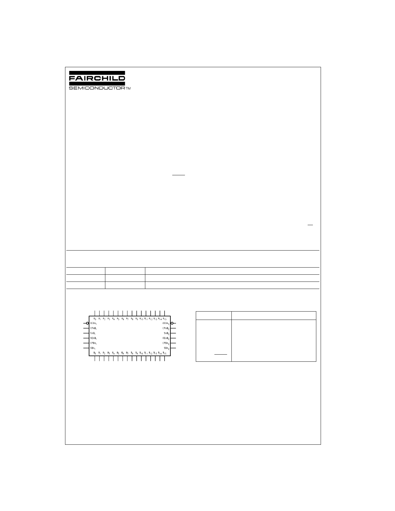
Logic Symbol
Pin Descriptions
Pin Names
Description
A0–A15
Data Register A Inputs/3-STATE Outputs
B0–B15
Data Register B Inputs/3-STATE Outputs
CPABn, CPBAn Clock Pulse Inputs
SABn, SBAn
Select Inputs
OEABn, OEBAn Output Enable Inputs
© 1999 Fairchild Semiconductor Corporation DS012005.prf
www.fairchildsemi.com
1 page 
Absolute Maximum Ratings(Note 3)
Symbol
Parameter
VCC Supply Voltage
VI DC Input Voltage
VO DC Output Voltage
IIK DC Input Diode Current
IOK DC Output Diode Current
IO
ICC
IGND
TSTG
DC Output Source/Sink Current
DC Supply Current per Supply Pin
DC Ground Current per Ground Pin
Storage Temperature
Value
−0.5 to +7.0
−0.5 to +7.0
−0.5 to +7.0
−0.5 to VCC + 0.5
−50
−50
+50
±50
±100
±100
−65 to +150
Conditions
Output in 3-STATE
Output in HIGH or LOW State (Note 4)
VI < GND
VO < GND
VO > VCC
Recommended Operating Conditions (Note 5)
Units
V
V
V
mA
mA
mA
mA
mA
°C
Symbol
Parameter
Min Max Units
VCC Supply Voltage
Operating
Data Retention
2.0
1.5
3.6
3.6
V
VI Input Voltage
VO Output Voltage
HIGH or LOW State
3-STATE
0
0
0
5.5
VCC
5.5
V
V
IOH/IOL Output Current
VCC = 3.0V − 3.6V
±24
VCC = 2.7V − 3.0V
±12 mA
VCC = 2.3V − 2.7V
±8
TA Free-Air Operating Temperature
−40 85
°C
∆t/∆V
Input Edge Rate, VIN = 0.8V–2.0V, VCC = 3.0V
0 10 ns/V
Note 3: The Absolute Maximum Ratings are those values beyond which the safety of the device cannot be guaranteed. The device should not be operated
at these limits. The parametric values defined in the Electrical Characteristics tables are not guaranteed at the Absolute Maximum Ratings. The “Recom-
mended Operating Conditions” table will define the conditions for actual device operation.
Note 4: IO Absolute Maximum Rating must be observed.
Note 5: Unused (inputs or I/O's) must be held HIGH or LOW. They may not float.
DC Electrical Characteristics
Symbol
Parameter
VIH HIGH Level Input Voltage
VIL LOW Level Input Voltage
VOH HIGH Level Output Voltage
VOL LOW Level Output Voltage
II Input Leakage Current
IOZ 3-STATE I/O Leakage
IOFF Power-Off Leakage Current
Conditions
IOH = −100 µA
IOH = −8 mA
IOH = −12 mA
IOH = −18 mA
IOH = −24 mA
IOL = 100 µA
IOL = 8 mA
IOL = 12 mA
IOL = 16 mA
IOL = 24 mA
0 ≤ VI ≤ 5.5V
0 ≤ VO ≤ 5.5V
VI = VIH or VIL
VI or VO = 5.5V
VCC
(V)
2.3 − 2.7
2.7 − 3.6
2.3 − 2.7
2.7 − 3.6
2.3 − 3.6
2.3
2.7
3.0
3.0
2.3 − 3.6
2.3
2.7
3.0
3.0
2.3 − 3.6
2.3 − 3.6
TA = −40°C to +85°C
Min Max
1.7
2.0
0.7
0.8
VCC − 0.2
1.8
2.2
2.4
2.2
0.2
0.6
0.4
0.4
0.55
±5.0
±5.0
0 10
Units
V
V
V
V
µA
µA
µA
5 www.fairchildsemi.com
5 Page | ||
| Páginas | Total 10 Páginas | |
| PDF Descargar | [ Datasheet 74LCX16652.PDF ] | |
Hoja de datos destacado
| Número de pieza | Descripción | Fabricantes |
| 74LCX16652 | Low Voltage Transceiver/Register with 5V Tolerant Inputs and Outputs | Fairchild Semiconductor |
| 74LCX16652MEA | Low Voltage Transceiver/Register with 5V Tolerant Inputs and Outputs | Fairchild Semiconductor |
| 74LCX16652MTD | Low Voltage Transceiver/Register with 5V Tolerant Inputs and Outputs | Fairchild Semiconductor |
| Número de pieza | Descripción | Fabricantes |
| SLA6805M | High Voltage 3 phase Motor Driver IC. |
Sanken |
| SDC1742 | 12- and 14-Bit Hybrid Synchro / Resolver-to-Digital Converters. |
Analog Devices |
|
DataSheet.es es una pagina web que funciona como un repositorio de manuales o hoja de datos de muchos de los productos más populares, |
| DataSheet.es | 2020 | Privacy Policy | Contacto | Buscar |