|
|
PDF TEA1102TS Data sheet ( Hoja de datos )
| Número de pieza | TEA1102TS | |
| Descripción | Fast charge ICs for NiCd/ NiMH/ SLA and LiIon | |
| Fabricantes | NXP Semiconductors | |
| Logotipo | ||
Hay una vista previa y un enlace de descarga de TEA1102TS (archivo pdf) en la parte inferior de esta página. Total 28 Páginas | ||
|
No Preview Available !
INTEGRATED CIRCUITS
DATA SHEET
TEA1102; TEA1102T;
TEA1102TS
Fast charge ICs for NiCd, NiMH,
SLA and LiIon
Preliminary specification
Supersedes data of 1997 Oct 09
File under Integrated Circuits, IC03
1999 Jan 27
1 page 
Philips Semiconductors
Fast charge ICs for NiCd, NiMH, SLA and
LiIon
Preliminary specification
TEA1102; TEA1102T;
TEA1102TS
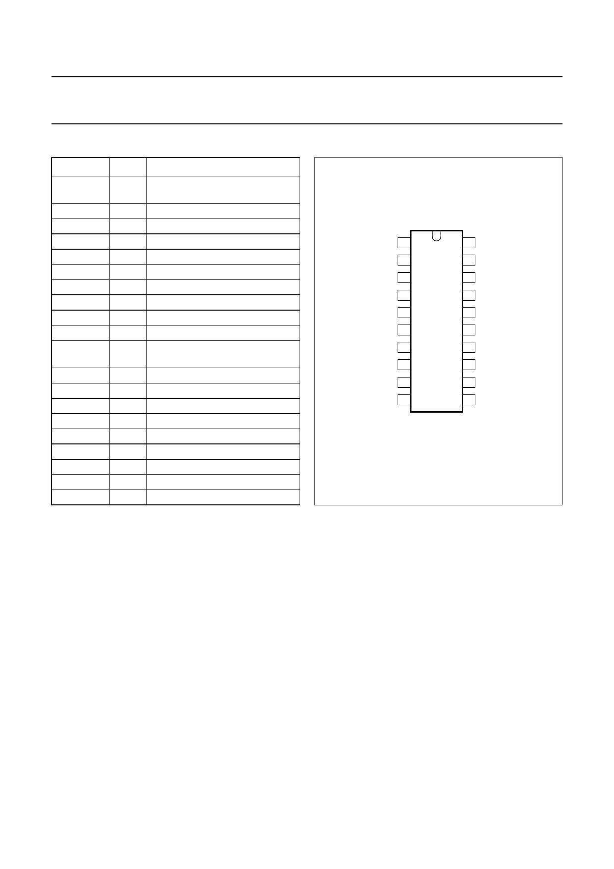
PINNING
SYMBOL
Vstb
IB
GND
PSD
LED
POD
PTD
NTC
MTV
RFSH
FCT
VP
Vsl
OSC
PWM
VS
LS
AO
Vbat
Rref
PIN DESCRIPTION
1 standby regulation voltage input
(NiCd and NiMH)
2 charge current setting
3 ground
4 program pin sample divider
5 LED output
6 program pin oscillator divider
7 program pin time-out divider
8 temperature sensing input
9 maximum temperature voltage
10 refresh input/output
11 fast charge termination and
battery chemistry identification
12 positive supply voltage
13 switched reference voltage output
14 oscillator input
15 pulse width modulator output
16 stabilized reference voltage
17 loop stability pin
18 analog output
19 single-cell battery voltage input
20 reference resistor pin
handbook, halfpage
Vstb 1
IB 2
GND 3
20 Rref
19 Vbat
18 AO
PSD 4
LED 5
POD 6
17 LS
16 VS
TEA1102
15 PWM
PTD 7
NTC 8
MTV 9
RFSH 10
14 OSC
13 Vsl
12 VP
11 FCT
MBH067
Fig.2 Pin configuration.
1999 Jan 27
5
5 Page 
Philips Semiconductors
Fast charge ICs for NiCd, NiMH, SLA and
LiIon
Preliminary specification
TEA1102; TEA1102T;
TEA1102TS
At an increase of the battery voltage the 14-bit
analog-to-digital convertor (ADC) is refreshed with this
new value. Therefore, the digitized value always
represents the maximum battery voltage. A decreased
Vbat voltage is not stored, but is compared to the stored
value.
Full is detected when the voltage decrease of Vbat is 1⁄4%
of the stored peak battery value. To avoid interference due
to the resistance of the battery contacts during battery
voltage sensing, the charge current is regulated to zero
during t = 210 × POD × tosc, via the regulation pins AO and
PWM. At the last period, the Vbat voltage is sensed and
stored in a sample-and-hold circuit. This approach
ensures very accurate detection of the battery full
condition (minus 1⁄4%).
When battery full is determined by ∆T/∆t, the voltage on
the NTC pin is used as the input voltage to the AD/DA
convertor. The sampling time at ∆T/∆t sensing is given by
the following equation:
ts
amplin
g
∆--∆---T-t-
=
217 × POD × PSD × tosc
(9)
After this initialized sample time the new temperature
voltage is compared to the preceding AD/DA voltage and
the AD/DA is refreshed with this new value. A certain
increase of the temperature is detected as full battery,
depending on the initialization settings. The decision of full
detection by ∆T/∆t or Vpeak is digitally filtered thus avoiding
false battery full detection.
Output drivers
The charge current regulation signal is available at two
output pins, AO and PWM.
ANALOG OUTPUT
The analog control voltage output at pin 18 (AO) can be
used to drive an opto-coupler in mains separated
applications when an external resistor is connected
between AO and the opto-coupler. The maximum current
through the opto-coupler diode is 2 mA. The voltage gain
of amplifier A2 is typical 11 dB (times 3.5). The DC voltage
transfer is given by the following equation:
Vao = 3.5 × (VLS − 1.35).
The AO output can be used for:
• Linear (DC) applications
• Not mains isolated SMPS with a separate controller
• Mains isolated SMPS, controlled by an opto-coupler.
PULSE WIDTH MODULATOR (PWM)
The LS voltage is compared internally with the oscillator
voltage to deliver a pulse width modulated output at PWM
(pin 15) to drive an output switching device in a SMPS
converter application via a driver stage. The PWM output
is latched to prevent multi-pulsing. The maximum duty
factor is internally fixed to 79% (typ.). The PWM output can
be used for synchronization and duty factor control of a
primary SMPS via a pulse transformer.
1999 Jan 27
11
11 Page | ||
| Páginas | Total 28 Páginas | |
| PDF Descargar | [ Datasheet TEA1102TS.PDF ] | |
Hoja de datos destacado
| Número de pieza | Descripción | Fabricantes |
| TEA1102T | Fast charge ICs for NiCd/ NiMH/ SLA and LiIon | NXP Semiconductors |
| TEA1102TS | Fast charge ICs for NiCd/ NiMH/ SLA and LiIon | NXP Semiconductors |
| Número de pieza | Descripción | Fabricantes |
| SLA6805M | High Voltage 3 phase Motor Driver IC. |
Sanken |
| SDC1742 | 12- and 14-Bit Hybrid Synchro / Resolver-to-Digital Converters. |
Analog Devices |
|
DataSheet.es es una pagina web que funciona como un repositorio de manuales o hoja de datos de muchos de los productos más populares, |
| DataSheet.es | 2020 | Privacy Policy | Contacto | Buscar |
