|
|
PDF VDP3108 Data sheet ( Hoja de datos )
| Número de pieza | VDP3108 | |
| Descripción | Single-Chip Video Processor | |
| Fabricantes | ETC | |
| Logotipo |  |
|
Hay una vista previa y un enlace de descarga de VDP3108 (archivo pdf) en la parte inferior de esta página. Total 30 Páginas | ||
|
No Preview Available !
MICRONAS
INTERMETALL
ADVANCE INFORMATION
VDP 3108
Single-Chip
Video Processor
Edition Oct. 12, 1994
6251-352-3AI
MICRONAS
1 page 
ADVANCE INFORMATION
VDP 3108
2. Functional Description
2.1.3. Automatic Gain Control
2.1. Analog Front End
This block provides the analog interfaces to all video in-
puts and mainly carries out analog-to digital conversion
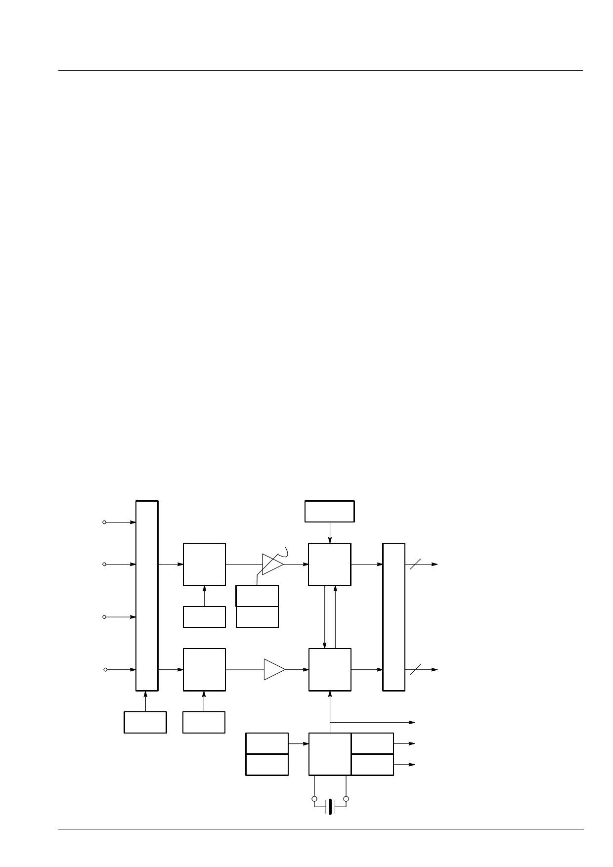
for the following digital video processing. A block dia-
gram is given in figure 2–1.
Most of the functional blocks in the front end are digitally
controlled (clamping, AGC and clock-DCO). The control
loops are closed by the Fast Processor (‘FP’) embedded
in the decoder.
2.1.1. Input Selector
Up to four analog inputs can be connected. Three inputs
are for input of composite video or S–VHS luma signal.
These inputs are clamped to the sync back porch and
are amplified by a variable gain amplifier. One input is
for connection of S–VHS carrier–chrominance signal.
This input is internally biased and has a fixed gain ampli-
fier.
2.1.2. Clamping
A digitally working automatic gain control adjusts the
magnitude of the selected baseband by +6/–4.5 dB in 64
logarithmic steps to the optimal range of the ADC .
The gain of the video input stage including the ADC is
213 steps/V for all three standards (PAL/NTSC/SECAM/
Y/C), with the AGC set to 0 dB.
2.1.4. Analog-to-Digital Converters
Two ADCs are provided to digitize the input signals.
Each converter runs with 20.25 MHz and has 8 bit reso-
lution. An integrated bandgap circuit generates the re-
quired reference voltages for the converters.
The two ADCs are of a 2-stage subranging type.
2.1.5. ADC Range
The ADC input range for the various input signals and
the digital representation is given in table 2–1 and figure
2–2.
The composite video input signals are AC coupled to the
IC. The clamping voltage is stored on the coupling ca-
pacitors and is generated by digitally controlled current
sources. The clamping level is the back porch of the vid-
eo signal. S-VHS chroma is also AC coupled. The input
pin is internally biased to the center of the ADC input
range.
2.1.6. Digitally Controlled Clock Oscillator
The clock generation is also a part of the analog front
end. The crystal oscillator is controlled digitally by the
control processor; the clock frequency can be adjusted
within ±150 ppm.
VIN3
CVBS/Y
reference
generation
AGC
+6/–4.5dB
VIN2
CVBS/Y
clamp
ADC
8 digital
CVBS
or Y
CVBS/ VIN1
Y/C
C CIN
level
DAC
gain
bias/
clamp
ADC
to
color
decod-
er
8 digital
chro-
ma
select
level
Fig. 2–1: Analog front end
DAC
freq.
DVC
O
± 150
ppm
frequ.
doubler
frequ.
divider
20.25
MHz
sys-
tem
clocks
MICRONAS INTERMETALL
5
5 Page 
ADVANCE INFORMATION
VDP 3108
2.2.9. Skew Filter
The system clock is free running and not locked to the
TV line frequency. Therefore, the ADC sampling pattern
is not orthogonal. The decoded YCrCb signals are con-
verted to an orthogonal sampling raster by skew filter
block at the output of the color decoder.
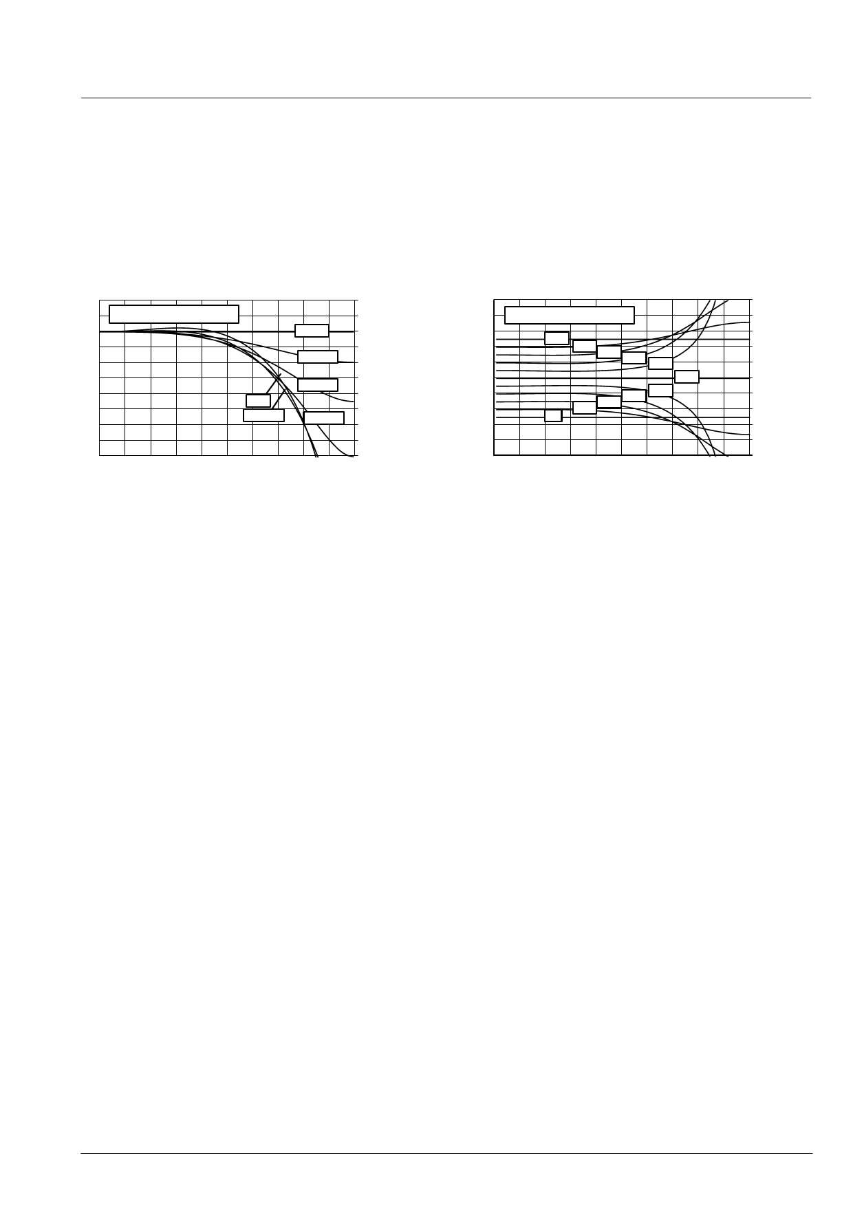
The skew filters are controlled by a skew parameter and
dB
2
1 parameter: α, 32 steps
0
–1
–2
–3
–4
–5
–6
–7
–8
0
2
4
0.5
0.4, 0.6
6
0, 1.0
0.1, 0.9
0.2, 0.8
0.3, 0.7
MHz
8 10
Fig. 2–11: Luminance, Chrominance skew
filter magnitude frequency response
allow to apply a group delay to the input signals without
introducing waveform of frequency response distortion.
The amount of phase shift of this filter is controlled by the
horizontal PLL1. The accuracy of the filters is 1/32
clocks for luminance and 1/4 clocks for chroma. Thus
the output of the color decoder is in an orthogonal pixel
format even in the case of nonstandard input signals
such as VCR.
clocks
2.5
2.3 parameter: α, 32 steps
2.1
1.0
1.9 0.9 0.8
1.7 0.7
1.5
0.6
1.3 0.3 0.4
1.1 0.1 0.2
0
0.9
0.7
0.5
02 4
6
0.5
8
MHz
10
Fig. 2–12: Luminance, chrominance skew
filter group delay characteristics
2.2.10. Picture Bus Color Space
Output of the color decoder block is YCrCb with 20.25
Msamples/s. Only active video is transferred. The num-
ber of active samples is 1068 per line for all standards
(525 lines and 625 lines).
The following equations explain the data formats. The
R,G,B source signals are already gamma-weighted.
The transform matrix from R,G,B to color difference sig-
nals is given by:
Y
ǒ Ǔ ǒ Ǔǒ ǓR*Y +
0.299 0.587 0.114 R
0.701 * 0.587 * 0.114 G
B*Y
* 0.299 * 0.587 0.886 B
In each TV broadcast standard different weighting fac-
tors for (R–Y) and (B–Y) are used:
PAL:
V = 0.877*(R–Y)
U = 0.493*(B–Y)
NTSC:
I = V*cos33° – U*sin33°
Q = V*sin33° + U*cos33°
SECAM: Dr = –1.9*(R–Y)
Db = 1.5*(B–Y)
MAC
Vm = 0.927*(R–Y)
Um = 0.733*(B–Y)
Studio
Cr = 0.713*(R–Y)
(CCIR 601) Cb = 0.564*(B–Y)
In the color decoder the weighting for both color differ-
ence signals is adjusted individually. The default format
will have the following specification:
Y = 224*Y + 16 (pure binary),
Cr = 224*(0.713*(R–Y)) + 128 (offset binary),
Cb = 224*(0.564*(B–Y)) + 128 (offset binary).
Optionally the picture bus format of the chrominance
components Cr, Cb can be switched to two’s comple-
ment format.
The YCrCb FIFO memories allow an adjustable delay for
the video processing e.g. one TV line. The memories are
controlled by the horizontal sync information available in
the front end and the display processor. Using the front
end sync, a window for the active video is generated.
Only active video data are written to the FIFO memories.
The display processor generates the main sync signal
from the display timing and data is read from the FIFOs
using the main sync signal. This allows an adjustable
delay as well as a variable delay, e.g. for VCR timebase
correction.
MICRONAS INTERMETALL
11
11 Page | ||
| Páginas | Total 30 Páginas | |
| PDF Descargar | [ Datasheet VDP3108.PDF ] | |
Hoja de datos destacado
| Número de pieza | Descripción | Fabricantes |
| VDP3104B | (VDP31xxB) Video Processor Family | Micronas Semiconductor |
| VDP3108 | Single-Chip Video Processor | ETC |
| VDP3108B | (VDP31xxB) Video Processor Family | Micronas Semiconductor |
| Número de pieza | Descripción | Fabricantes |
| SLA6805M | High Voltage 3 phase Motor Driver IC. |
Sanken |
| SDC1742 | 12- and 14-Bit Hybrid Synchro / Resolver-to-Digital Converters. |
Analog Devices |
|
DataSheet.es es una pagina web que funciona como un repositorio de manuales o hoja de datos de muchos de los productos más populares, |
| DataSheet.es | 2020 | Privacy Policy | Contacto | Buscar |
