|
|
PDF V29C51400T Data sheet ( Hoja de datos )
| Número de pieza | V29C51400T | |
| Descripción | 4 MEGABIT 262/144 x 16 BIT/524/288 x 8 BIT 5 VOLT CMOS FLASH MEMORY | |
| Fabricantes | Mosel Vitelic Corp | |
| Logotipo |  |
|
Hay una vista previa y un enlace de descarga de V29C51400T (archivo pdf) en la parte inferior de esta página. Total 16 Páginas | ||
|
No Preview Available !
MOSEL VITELIC
V29C51400T/V29C51400B
4 MEGABIT
(262,144 x 16 BIT/524,288 x 8 BIT)
5 VOLT CMOS FLASH MEMORY
PRELIMINARY
Features
s 256K x 16-bit or 512K x 8-bit Organization
s Address Access Time: 70, 90, 120 ns
s Single 5V ± 10% Power Supply
s Sector Erase Mode Operation
s 16KB Boot Block (lockable)
s 1K bytes per Sector, 512 Sectors
– Sector-Erase Cycle Time: 10ms (Max)
– Byte-Write Cycle Time: 20µs (Max)
s Minimum 10,000 Erase-Program Cycles
s Low power dissipation
– Active Read Current: 19mA (Typ)
– Active Program Current: 30mA (Typ)
– Standby Current: 100µA (Max)
s Hardware Data Protection
s Low VCC Program Inhibit Below 3.5V
s Self-timed write/erase operations with end-of-
cycle detection
– DATA Polling
– Toggle Bit
s CMOS and TTL Interface
s Available in two versions
– V29C51400T (Top Boot Block)
– V29C51400B (Bottom Boot Block)
s Packages:
– 48-pin TSOP
Description
The V29C51400T/V29C51400B is a high speed
262,144 x 16 bit or 524,288 x 8-bit CMOS flash
memory. Writing or erasing the device is done with
a single 5 Volt power supply. The device has
separate chip enable CE, write enable WE, and
output enable OE controls to eliminate bus
contention.
The V29C51400T/V29C51400B offers a combi-
nation of: Boot Block with Sector Erase/Write
Mode. The end of write/erase cycle is detected by
DATA Polling of I/O7 or by the Toggle Bit I/O6.
The V29C51400T/V29C51400B features a
sector erase operation which allows each sector to
be erased and reprogrammed without affecting
data stored in other sectors. The device also
supports full chip erase.
Boot block architecture enables the device to
boot from a protected sector located either at the
top (V29C51400T) or the bottom (V29C51400B).
All inputs and outputs are CMOS and TTL
compatible.
The V29C51400T/V29C51400B is ideal for
applications that require updatable code and data
storage.
Device Usage Chart
Operating
Temperature
Range
0°C to 70 °C
Package Outline
T
•
Access Time (ns)
70 90 120
•••
Temperature
Mark
Blank
V29C51400T/V29C51400B Rev. 1.5 October 2000
1
1 page 
MOSEL VITELIC
V29C51400T/V29C51400B
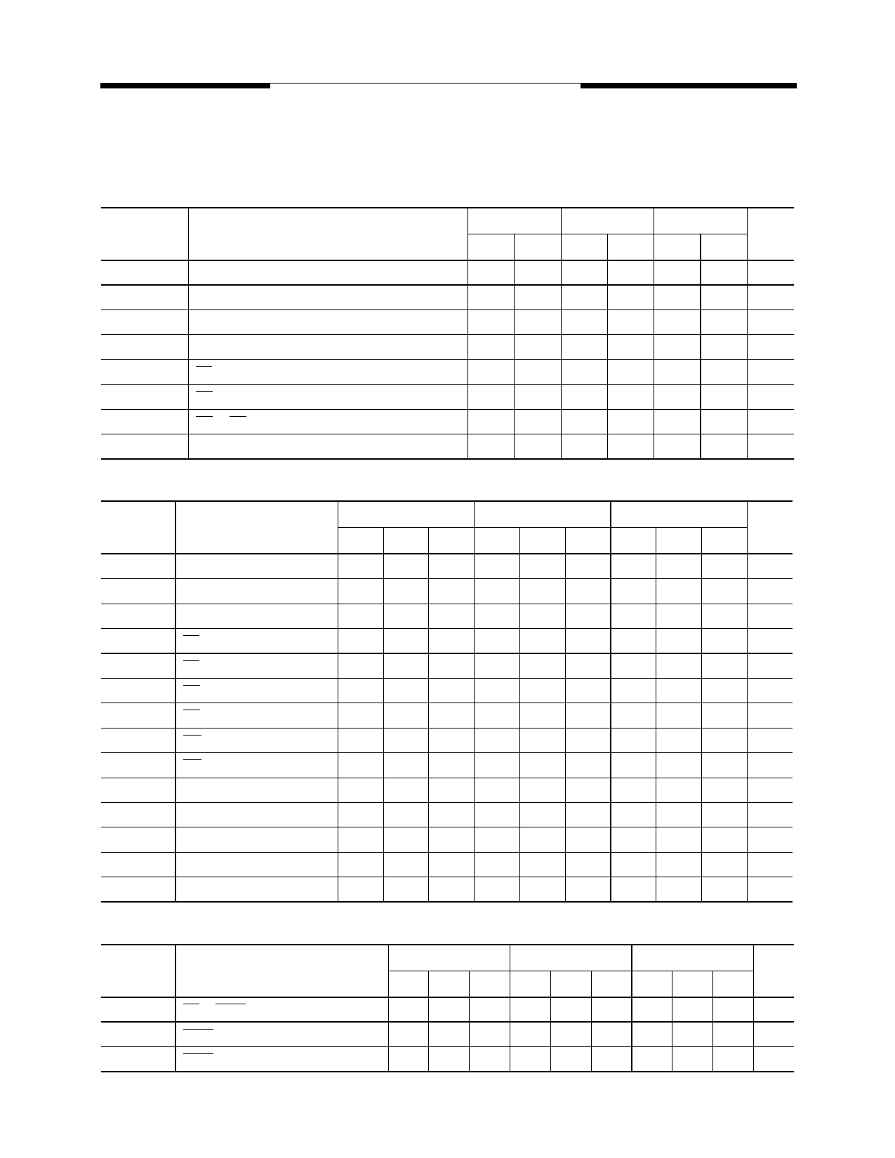
AC Electrical Characteristics
(over all temperature ranges)
Read Cycle
Parameter
Name
tRC
tAA
tACS
tOE
tCLZ
tOLZ
tDF
tOH
Parameter
Read Cycle Time
Address Access Time
Chip Enable Access Time
Output Enable Access Time
CE Low to Output Active
OE Low to Output Active
OE or CE High to Output in High Z
Output Hold from Address Change
-70
Min. Max.
70 —
— 70
— 70
— 35
0—
0—
0 20
0—
-90
Min. Max.
90 —
— 90
— 90
— 45
0—
0—
0 20
0—
-12
Min. Max.
120 —
— 120
— 120
— 60
0—
0—
0 30
0—
Unit
ns
ns
ns
ns
ns
ns
ns
ns
Program (Erase/Program) Cycle
Parameter
Name Parameter
tWC
tAS
tAH
tCS
tCH
tOES
tOEH
tWP
tWPH
tDS
tDH
tWHWH1
tWHWH2
tWHWH3
Write Cycle Time
Address Setup Time
Address Hold Time
CE Setup Time
CE Hold Time
OE Setup Time
OE High Hold Time
WE Pulse Width
WE Pulse Width High
Data Setup Time
Data Hold Time
Programming Cycle
Sector Erase Cycle
Chip Erase Cycle
Min.
70
0
45
0
0
0
0
35
20
30
0
—
—
—
-70
Typ.
—
—
—
—
—
—
—
—
—
—
—
—
—
2
Max.
—
—
—
—
—
—
—
—
—
—
—
20
10
—
Min.
90
0
45
0
0
0
0
45
30
30
0
—
—
—
-90
Typ.
—
—
—
—
—
—
—
—
—
—
—
—
—
2
Max.
—
—
—
—
—
—
—
—
—
—
—
20
10
—
Min.
120
0
50
0
0
0
0
50
35
30
0
—
—
—
-12
Typ.
—
—
—
—
—
—
—
—
—
—
—
—
—
2
Max.
—
—
—
—
—
—
—
—
—
—
—
20
10
—
Unit
ns
ns
ns
ns
ns
ns
ns
ns
ns
ns
ns
µs
ms
sec
Word/Byte Configuration
Parameter
Name Parameter
tELFL/tELFH
tFLQZ
tFHQV
CE to BYTE Switching Low/High
BYTE Low to Output in HIGH
BYTE High to Output Active
-70 -90 -12
Min. Typ. Max. Min. Typ. Max. Min. Typ. Max. Unit
— — 5 — — 5 — — 5 ns
— — 20 — — 20 — — 30 ns
70 — — 90 — — 120 — — ns
V29C51400T/V29C51400B Rev. 1.5 October 2000
5
5 Page 
MOSEL VITELIC
V29C51400T/V29C51400B
Sector Erase Cycle
The V29C51400T/V29C51400B features a sector
erase operation which allows each sector to be
erased and reprogrammed without affecting data
stored in other sectors. Sector erase operation is
initiated by using a specific six-bus-cycle sequence:
Two unlock program cycles, a setup command, two
additional unlock program cycles, and the sector
erase command (see Table 2). A sector must be first
erased before it can be re-written. While in the
internal erase mode, the device ignores any
program attempt into the device. The internal erase
completion can be determined via DATA polling or
toggle bit status.
The V29C51400T/V29C51400B is shipped fully
erased (all bits = 1).
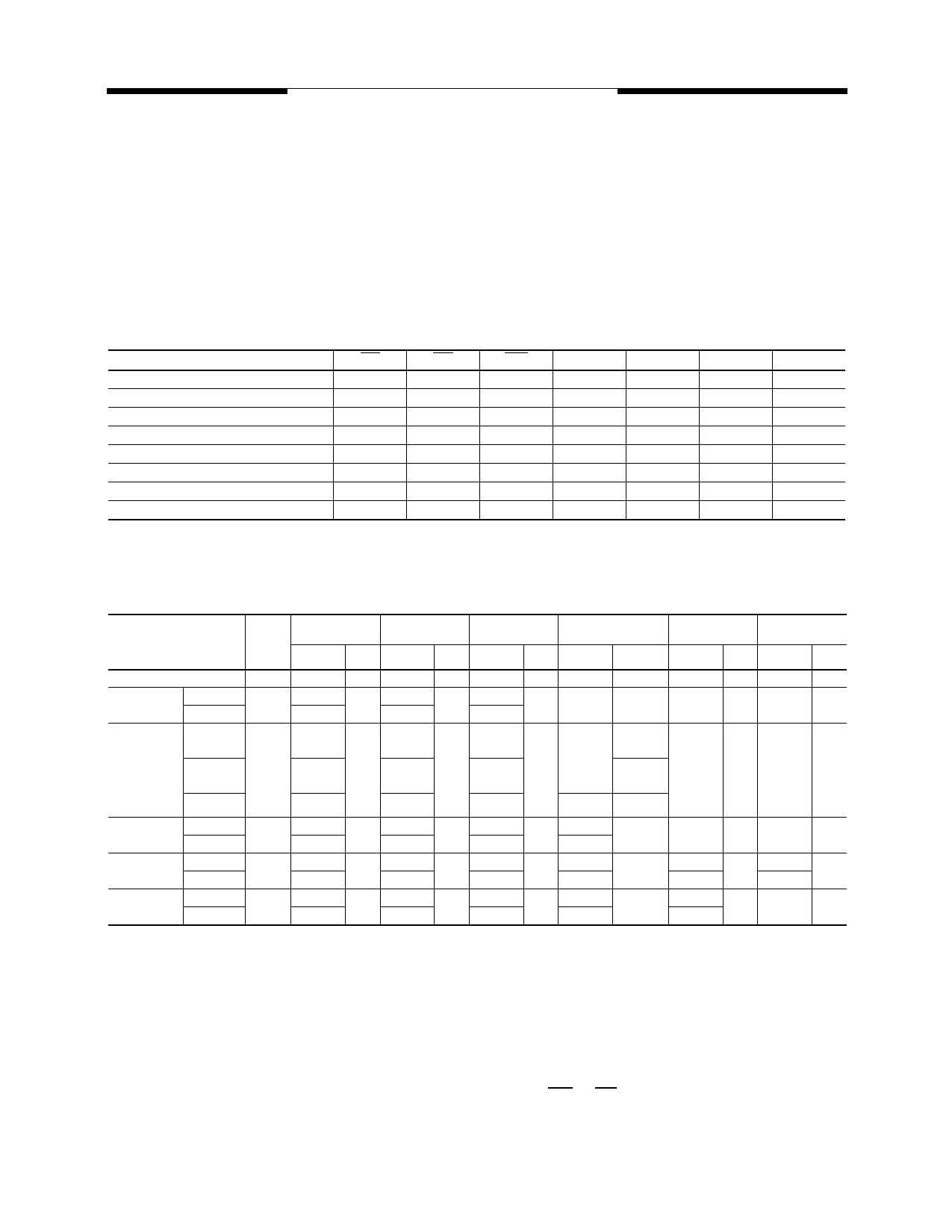
Table 1. Operation Modes Decoding
Decoding Mode
CE OE WE A0 A1 A9 I/O
Read
VIL VIL VIH A0 A1 A9 READ
Byte Write
VIL VIH VIL A0 A1 A9 PD
Standby
VIH X X X X X HIGH-Z
Autoselect Device ID
VIL VIL VIH VIH VIL VH CODE
Autoselect Manufacture ID
VIL VIL VIH VIL VIL VH CODE
Enabling Boot Block Protection Lock
VIL
VH
VIL
X
X VH X
Disabling Boot Block Protection Lock
VH
VH
VIL
X
X VH X
Output Disable
VIL VIH VIH
X
X
X HIGH-Z
NOTES:
1. X = Don’t Care, VIH = HIGH, VIL = LOW, VH = 12.5V Max.
2. PD: The data at the byte address to be programmed.
Table 2. Command Codes
Command
Sequence
Reset/Read
Reset/Read
Autoselect
Mode
Program
Chip Erase
Sector Erase
Word
Byte
Word
Bus
Write
Cycles
Req’d
1
3
3
Byte
Word/Byte
Word
Byte
Word
Byte
Word
Byte
4
0
6
First Bus
Program Cycle
Address Data
XXXXH F0H
5555H AAH
AAAAH
5555H AAH
AAAAH
5555H
AAAAH
5555H
AAAAH
5555H
AAAAH
AAH
AAH
AAH
Second Bus
Program Cycle
Address Data
2AAAH
5555H
2AAAH
55H
55H
5555H
2AAAH
5555H
2AAAH
5555H
2AAAH
5555H
55H
55H
55H
Third Bus
Program Cycle
Address Data
5555H
AAAAH
5555H
F0H
90H
AAAAH
5555H
AAAAH
5555H
AAAAH
5555H
AAAAH
A0H
80H
80H
Fourth Bus
Program Cycle
Address Data
Fifth Bus
Program Cycle
Address Data
RA RD
01H
00H
PA
13H, B3H
(B Device
ID)
13H, B3H
(B Device
ID)
40H
(Manuf. ID)
PD(4)
5555H
AAAAH
5555H
AAAAH
AAH
AAH
2AAAH
5555H
2AAAH
5555H
55H
55H
Six Bus
Program Cycle
Address Data
5555H
AAAAH
SA
10H
30H
NOTES:
1. RA: Read Address
2. RD: Read Data
3. PA: The address of the memory location to be programmed.
4. PD: The data at the byte address to be programmed.
5. SA(5): Sector Address
Chip Erase Cycle
The V29C51400T/V29C51400B features a chip-
erase operation. The chip erase operation is
initiated by using a specific six-bus-cycle
sequence: two unlock program cycles, a setup
command, two additional unlock program cycles,
and the chip erase command (see Table 2).
The automatic erase begins on the rising edge of
the last WE or CE pulse in the command sequence
and terminates when the data on DQ7 is “1”.
V29C51400T/V29C51400B Rev. 1.5 October 2000
11
11 Page | ||
| Páginas | Total 16 Páginas | |
| PDF Descargar | [ Datasheet V29C51400T.PDF ] | |
Hoja de datos destacado
| Número de pieza | Descripción | Fabricantes |
| V29C51400B | 4 MEGABIT 262/144 x 16 BIT/524/288 x 8 BIT 5 VOLT CMOS FLASH MEMORY | Mosel Vitelic Corp |
| V29C51400T | 4 MEGABIT 262/144 x 16 BIT/524/288 x 8 BIT 5 VOLT CMOS FLASH MEMORY | Mosel Vitelic Corp |
| Número de pieza | Descripción | Fabricantes |
| SLA6805M | High Voltage 3 phase Motor Driver IC. |
Sanken |
| SDC1742 | 12- and 14-Bit Hybrid Synchro / Resolver-to-Digital Converters. |
Analog Devices |
|
DataSheet.es es una pagina web que funciona como un repositorio de manuales o hoja de datos de muchos de los productos más populares, |
| DataSheet.es | 2020 | Privacy Policy | Contacto | Buscar |
