|
|
|
PDF VS3V257QX Data sheet ( Hoja de datos )
| Número de pieza | VS3V257QX | |
| Descripción | High-speed 3.3V CMOS VSwitch Quad 2:1 Mux/Demux | |
| Fabricantes | Vaishali Semiconductor | |
| Logotipo | ||
Hay una vista previa y un enlace de descarga de VS3V257QX (archivo pdf) en la parte inferior de esta página. Total 6 Páginas | ||
|
No Preview Available !
VS3V257 / VS3V2257
High-speed 3.3V CMOS VSwitch
Quad 2:1 Mux/Demux
Applications
•= 3.3V to 2.5V translation
•= 2.5V to 1.8V translation
•= Hot-Swapping
•= Logic replacement
•= Memory bank, video, and audio
switching
General Description
The VS3V257 is a high-speed LVTTL–compatible Quad 2:1 multiplexer/demultiplexer. The VS3V257
contains four mux/demux channels, with a common path control (S) and active low enable (/E). The low ON
resistance of the VS3V257 allows inputs to be connected to outputs, without adding propagation delay and
without generating additional signal noise. The VS3V2257 has 25Ω resistors in series with the switches to
reduce ground-bounce noise and signal reflection.
The VS3V257 and VS3V2257 are designed for 3.3V to 2.5V or 2.5V to 1.8V level translation, without any
external components. These switches also offer very high impedance between switch terminals in the
power-off or “disabled” state. This feature, combined with near-zero propagation delay in the “on” state,
makes VS3V257 and VS3V2257 ideal interface elements for hot-swapping applications.
Features
•= Enhanced N-FET with no DC path to VCC
or GND in normal operating signal voltage
range.
•= Low impedance switches connect inputs to
outputs with near-zero propagation delay:
5Ω (VS3V257) and 25Ω (VS3V2257)
•= Pin-compatible with 74LVC257 or
equivalent logic devices
•= Zero added ground bounce or signal noise
•= Break-before-make feature
•= Undershoot clamp diodes on all switch and
control pins
•= ESD rating >2000V (Human Body Model)
•= or >200V (Machine Model)
•= Latch-up current >100mA
•= Available in 150-mil wide QSOP package
Figure 1. Functional Block Diagram
Figure 2. Pin Configuration
S
/E
YA
YB
YC
YD
QSOP
I0A
I1A
I0B
I1B
I0C
I1C
I0D
I1D
S
I0A
I1A
YA
I0B
I1B
YB
GND
1
2
3
4
5
6
7
8
16 VCC
15 /E
14 I0D
13 I1D
12 YD
11 I0C
10 I1C
9 YC
(All Pins Top View)
2000-11-28
Page 1
MDSS-0001-01
www.vaishali.com
Vaishali Semiconductor 747 Camden Avenue, Suite C Campbell CA 95008 Ph. 408.377.6060 Fax 408.377.6063
1 page 
VS3V257/VS3V2257
Table 8. Switching Characteristics Over Operating Range – 3.3V Supply Voltage
TA = -40oC to +85oC, VCC = 3.3V + 0.3V
CLOAD = 30pF, RLOAD = 1kΩ unless otherwise stated.
Symbol
tPLH, tPHL
Description (1)
Data Propagation Delay (2,3) through the switch
VS3V257
Min(3) Max
0.25
VS3V2257
Min(3) Max
1.25
tPZH, tPZL
Switch Turn-on Delay, S to YX, I0X, or I1X
0.5 5.2 0.5 6.2
tPZH, tPZL
Switch Turn-on Delay, /E to YX, I0X, or I1X
0.5 4.8 0.5 5.8
tPLZ, tPHZ
Switch Turn-off Delay (3), S or /E to YX, I0X, or I1X
0.5
5.0
0.5 5.0
Units
ns
ns
ns
ns
Table 9. Switching Characteristics Over Operating Range – 2.5V Supply Voltage
TA = -40oC to +85oC, VCC = 2.5V + 0.2V
CLOAD = 30pF, RLOAD = 1kΩ unless otherwise stated.
Symbol
tPLH, tPHL
Description (1)
Data Propagation Delay (2,3) through the switch
VS3V257
Min(3) Max
VS3V2257
Min(3) Max
tPZH, tPZL
Switch Turn-on Delay, S to YX, I0X, or I1X
tPZH, tPZL
Switch Turn-on Delay, /E to YX, I0X, or I1X
tPLZ, tPHZ
Switch Turn-off Delay (3), S or /E to YX, I0X, or I1X
Units
ns
ns
ns
ns
Notes:
1. See test circuits and waveforms.
2. This parameter is the calculated theoretical RC time constant of ON-state resistance of the switch and the
specified load capacitance when driven by an ideal voltage source (zero source impedance). This time-constant is
on the order of 0.25 ns for VS3V257 and 1.25 ns for VS3V2257. Since this time-constant is much smaller than
rise/fall times of typical driving signals, it adds very little propagation delay to the system.
3. This parameter is guaranteed, but not production tested.
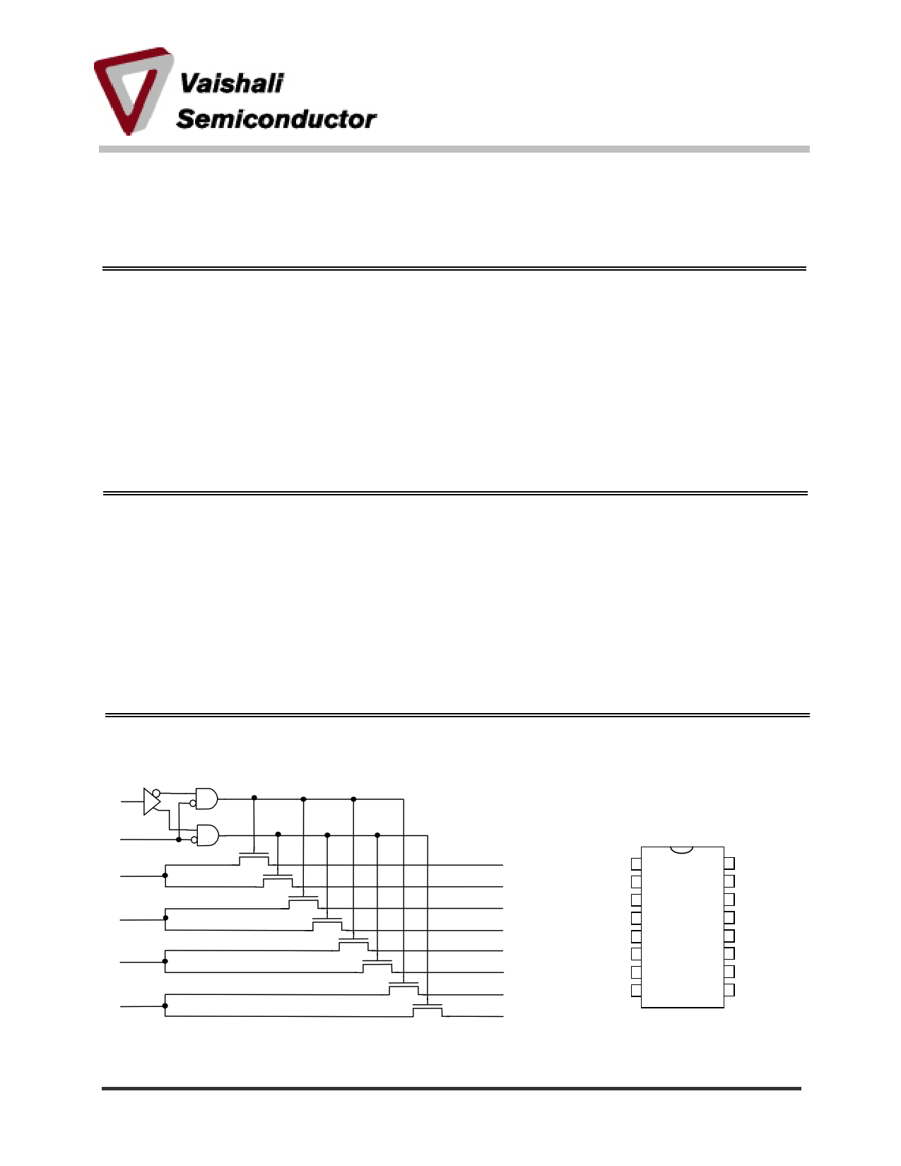
Figure 7. AC Test Circuit and Switching Waveforms
AC Test Circuit 3.3V Supply Voltage
Pulse
Generator
VIN VOUT
DUT
50Ω
CL
S1
5V
R1
1k Ω
950Ω
RL
50Ω=Coax to
Oscilloscope
Load Switch Position
TEST
tPLH, tPHL
tPLZ, tPZL
tPHZ, tPZH
S1
Open
5V
GND
Input Conditions
Input voltage = 0 V to 3.0 V
tr = tf = 2.5ns (10% to 90%)
2000-11-28
Page 5
MDSS-0001-01
www.vaishali.com
Vaishali Semiconductor 747 Camden Avenue, Suite C Campbell CA 95008 Ph. 408.377.6060 Fax 408.377.6063
5 Page | ||
| Páginas | Total 6 Páginas | |
| PDF Descargar | [ Datasheet VS3V257QX.PDF ] | |
Hoja de datos destacado
| Número de pieza | Descripción | Fabricantes |
| VS3V257Q | High-speed 3.3V CMOS VSwitch Quad 2:1 Mux/Demux | Vaishali Semiconductor |
| VS3V257QX | High-speed 3.3V CMOS VSwitch Quad 2:1 Mux/Demux | Vaishali Semiconductor |
| Número de pieza | Descripción | Fabricantes |
| SLA6805M | High Voltage 3 phase Motor Driver IC. |
Sanken |
| SDC1742 | 12- and 14-Bit Hybrid Synchro / Resolver-to-Digital Converters. |
Analog Devices |
|
DataSheet.es es una pagina web que funciona como un repositorio de manuales o hoja de datos de muchos de los productos más populares, |
| DataSheet.es | 2020 | Privacy Policy | Contacto | Buscar |