|
|
|
PDF XM28C040M-20 Data sheet ( Hoja de datos )
| Número de pieza | XM28C040M-20 | |
| Descripción | 5 Volt/ Byte Alterable E2PROM | |
| Fabricantes | Xicor Inc. | |
| Logotipo | ||
Hay una vista previa y un enlace de descarga de XM28C040M-20 (archivo pdf) en la parte inferior de esta página. Total 17 Páginas | ||
|
No Preview Available !
XM28C040
4 Megabit Module
XM28C040
5 Volt, Byte Alterable E2PROM
512K x 8 Bit
TYPICAL FEATURES
• High Density 4 Megabit (512K x 8) Module
• Access Time of 200ns at –55°C to +125°C
• Base Memory Component: Xicor X28C010
• Pinout Conforms to JEDEC Standard for
4 Megabit E2PROM
• Fast Write Cycle Times
—256 Byte Page Write
• Early End of Write Detection
—DATA Polling
—Toggle Bit Polling
• Software Data Protection
• Three Temperature Ranges
—Commercial: 0°C to +75°C
—Industrial: –40° to +85°C
—Military: –55° to +125°C
• High Rel Modules all Components are
MIL-STD-883 Compliant
• Endurance: 100,000 Cycles
DESCRIPTION
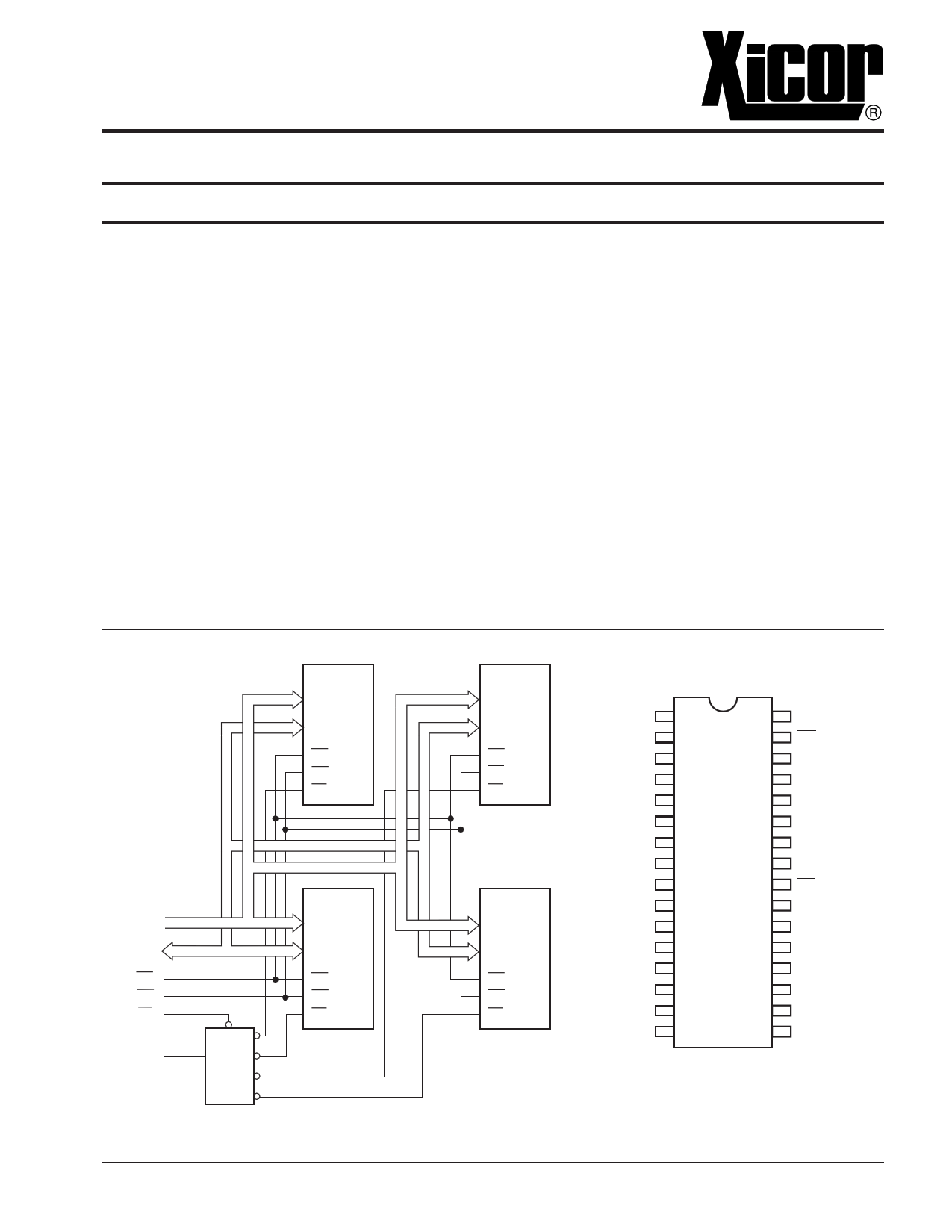
The XM28C040 is a high density 4 Megabit E2PROM
comprised of four X28C010's mounted on a co-fired
multilayered ceramic substrate. Individual components
are 100% tested prior to assembly in module form and
then 100% tested after assembly.
The XM28C040 is configured 512K x 8 bit. The module
supports a 256-byte page write operation. This com-
bined with DATA Polling or Toggle Bit Polling, effectively
provides a 39µs/byte write cycle, enabling the entire
array to be rewritten in 10 seconds.
The XM28C040 provides the same high endurance and
data retention as the X28C010.
FUNCTIONAL DIAGRAM
X28C010
A0–A16
I/O0–I/O7
OE
WE
CE
A0–A16
I/O0–I/O7
OE
WE
CE
A18
A17
X28C010
A0–A16
I/O0–I/O7
OE
WE
CE
X28C010
A0–A16
I/O0–I/O7
OE
WE
CE
X28C010
A0–A16
I/O0–I/O7
OE
WE
CE
PIN CONFIGURATION
A18
A16
A15
A12
A7
A6
A5
A4
A3
A2
A1
A0
I/O0
I/O1
I/O2
VSS
1 32
2 31
3 30
4 29
5 28
6 27
7 26
8 25
XM28C040
9 24
10 23
11 22
12 21
13 20
14 19
15 18
16 17
VCC
WE
A17
A14
A13
A8
A9
A11
OE
A10
CE
I/O7
I/O6
I/O5
I/04
I/O3
3873 FHD F02
© Xicor, Inc. 1991-1997 Patents Pending
3873-1.7 6/13/97 T1/C0/D0 SH
3873 FHD F01
1
Characteristics subject to change without notice
1 page 
XM28C040
THE TOGGLE BIT I/O6
Figure 4. Toggle Bit Bus Sequence
LAST
WE WRITE
CE
OE
I/O6
VOH
*
VOL
* Beginning and ending state of I/O6 will vary.
Figure 5. Toggle Bit Software Flow
LAST WRITE
LOAD ACCUM
FROM ADDR n
COMPARE
ACCUM WITH
ADDR n
HIGH Z
*
READY
3873 FHD F12
The Toggle Bit can eliminate the software housekeeping
chore of saving and fetching the last address and data
written to a device in order to implement DATA Polling.
This can be especially helpful in an array comprised of
multiple XM28C040 memories that is frequently up-
dated. The timing diagram in Figure 4 illustrates the
sequence of events on the bus. The software flow
diagram in Figure 5 illustrates a method for testing the
Toggle Bit.
COMPARE
OK?
YES
READY
NO
3873 FHD F13
5
5 Page 
XM28C040
A.C. CONDITIONS OF TEST
MODE SELECTION
Input Pulse Levels
0V to 3V
CE OE WE
Mode
Input Rise and
L L H Read
Fall Times
10ns
L H L Write
Input and Output
Timing Levels
1.5V
H X X Standby and Write Inhibit
X L X Write Inhibit
Output Load
1 TTL Gate and
CL = 100pF
X X H Write Inhibit
3873 PGM T05.1
A.C. CHARACTERISTICS
XM28C040 TA = 0°C to +75°C, VCC = +5V ±10%, unless otherwise specified.
XM28C040I TA = –40°C to +85°C, VCC = +5V ±10%, unless otherwise specified.
XM28C040M TA = –55°C to +125°C, VCC = +5V ±10%, unless otherwise specified.
Read Cycle Limits
I/O
DOUT
DIN
High Z
—
—
Power
Active
Active
Standby
—
—
3873 PGM T06
XM28C040-20 XM28C040-25 XM28C040
Symbol
tRC
tCE
tAA
tOE
tLZ(4)
tOLZ(4)
tHZ(4)
tOHZ(4)
tOH
Parameter
Read Cycle Time
Chip Enable Access Time
Address Access Time
Output Enable Access Time
CE Low to Active Output
OE Low to Active Output
CE High to High Z Output
OE High to High Z Output
Output Hold From Address Change
Min.
200
0
0
0
Read Cycle
Max.
200
200
80
100
100
Min.
250
0
0
0
Max.
250
250
100
100
100
Min.
300
0
0
0
Max.
300
300
100
100
100
Units
ns
ns
ns
ns
ns
ns
ns
ns
ns
3873 PGM T07
tRC
ADDRESS
tCE
CE
tOE
OE
VIH
WE
DATA I/O
HIGH Z
tOLZ
tLZ
DATA VALID
tOH
tHZ
DATA VALID
tOHZ
tAA
3873 FHD F03
Note: (3) tHZ and tOHZ are measured from the point when CE or OE return high (whichever occurs first) to the time when the outputs are
no longer driven.
11
11 Page | ||
| Páginas | Total 17 Páginas | |
| PDF Descargar | [ Datasheet XM28C040M-20.PDF ] | |
Hoja de datos destacado
| Número de pieza | Descripción | Fabricantes |
| XM28C040M-20 | 5 Volt/ Byte Alterable E2PROM | Xicor Inc. |
| XM28C040M-25 | 5 Volt/ Byte Alterable E2PROM | Xicor Inc. |
| Número de pieza | Descripción | Fabricantes |
| SLA6805M | High Voltage 3 phase Motor Driver IC. |
Sanken |
| SDC1742 | 12- and 14-Bit Hybrid Synchro / Resolver-to-Digital Converters. |
Analog Devices |
|
DataSheet.es es una pagina web que funciona como un repositorio de manuales o hoja de datos de muchos de los productos más populares, |
| DataSheet.es | 2020 | Privacy Policy | Contacto | Buscar |