|
|
|
PDF ADM1275 Data sheet ( Hoja de datos )
| Número de pieza | ADM1275 | |
| Descripción | Hot-Swap Controller and Digital Power Monitor | |
| Fabricantes | Analog Devices | |
| Logotipo | ||
Hay una vista previa y un enlace de descarga de ADM1275 (archivo pdf) en la parte inferior de esta página. Total 30 Páginas | ||
|
No Preview Available !
Data Sheet
Hot-Swap Controller and Digital Power
Monitor with PMBus Interface
ADM1275
FEATURES
Controls supply voltages from 2 V to 20 V
370 ns response time to short circuit
Resistor-programmable 5 mV to 25 mV current limit
±1% accurate, 12-bit ADC for current, VIN/VOUT readback
Charge-pumped gate drive for multiple external N-channel FETs
High gate drive voltage to ensure lowest RDSON
Foldback for tighter FET SOA protection
Automatic retry or latch-off on current fault
Programmable current limit timer for SOA
Programmable, multifunction GPOs
Power-good status output
Analog UV and OV protection
ENABLE pin (ADM1275-3 only)
Peak detect registers for current and voltage
PMBus fast mode compliant interface
16-lead QSOP and 20-lead QSOP and LFCSP
APPLICATIONS
Power monitoring and control/power budgeting
Central office equipment
Telecommunication and data communication equipment
PCs/servers
GENERAL DESCRIPTION
The ADM1275 is a hot-swap controller that allows a circuit board
to be removed from or inserted into a live backplane. It also features
current and voltage readback via an integrated 12-bit analog-to-
digital converter (ADC), accessed using a PMBus™ interface.
The load current is measured using an internal current sense
amplifier that measures the voltage across a sense resistor in
the power path via the SENSE+ and SENSE− pins. A default
limit of 20 mV is set, but this limit can be adjusted, if required,
using a resistor divider network from the internal reference
voltage to the ISET pin.
The ADM1275 limits the current through the sense resistor by
controlling the gate voltage of an external N-channel FET in the
power path, via the GATE pin. The sense voltage—and, therefore,
the load current—is maintained below the preset maximum. The
ADM1275 protects the external FET by limiting the time that the
FET remains on while the current is at its maximum value. This
current limit time is set by the choice of capacitor connected to
the TIMER pin. In addition, a foldback resistor network can be
used to actively lower the current limit as the voltage across the
FET is increased. This helps to maintain constant power in the
FET and allows the safe operating area (SOA) to be adhered to
in an effective manner.
Rev. D
Document Feedback
Information furnished by Analog Devices is believed to be accurate and reliable. However, no
responsibility is assumed by Analog Devices for its use, nor for any infringements of patents or other
rights of third parties that may result from its use. Specifications subject to change without notice. No
license is granted by implication or otherwise under any patent or patent rights of Analog Devices.
Trademarksandregisteredtrademarksarethepropertyoftheirrespectiveowners.
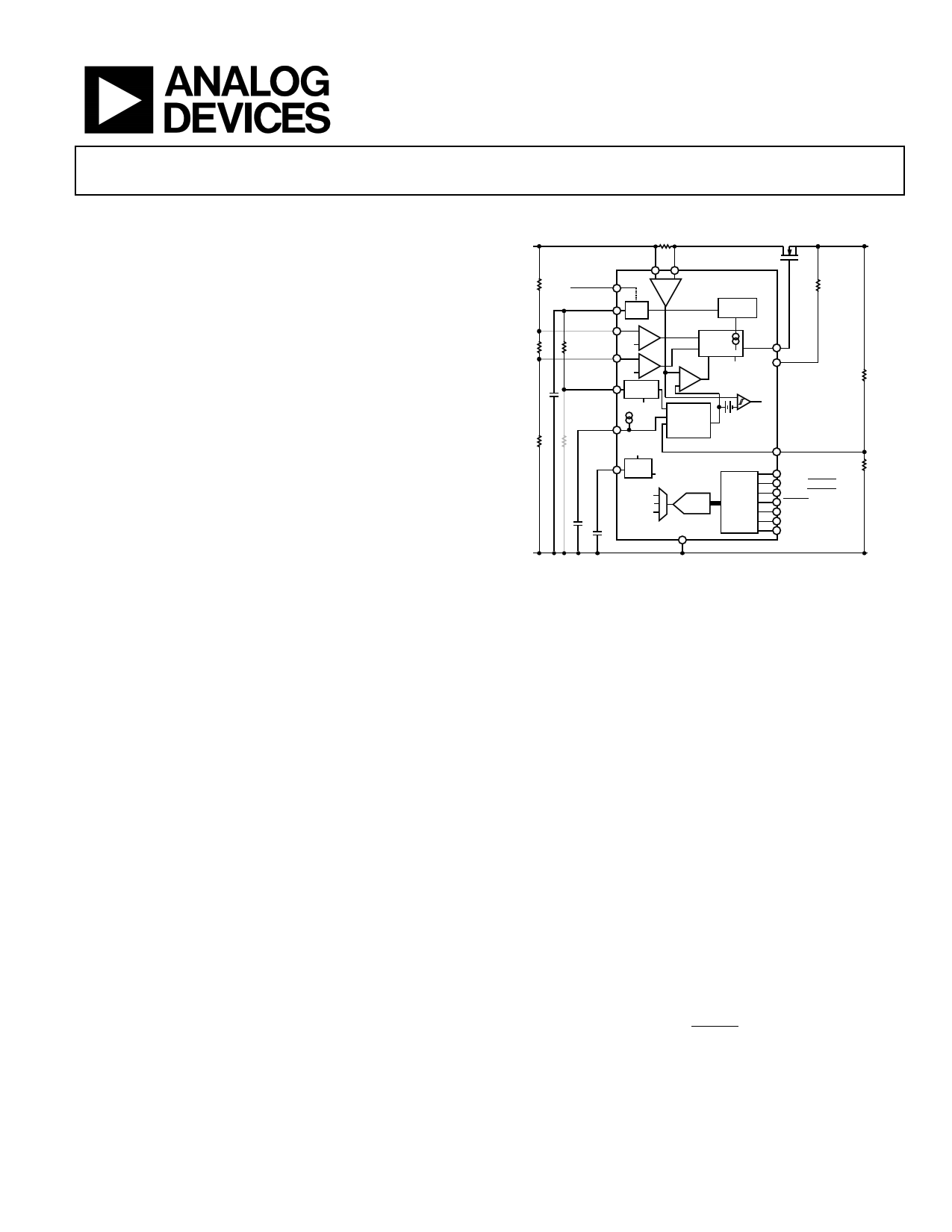
2V TO 20V
APPLICATIONS DIAGRAM
RSENSE
Q1
2.95V
SENSE+
SENSE–
TO
20V VCC
+×50–
ADM1275-1
VCAP LDO
UV
+
1.0V –
OV
–
1.0V +
ISET
REF
SELECT
1.0V
SS
IOUT
+
–
CHARGE
PUMP
VCP
GATE
DRIVE/
LOGIC
TIMEOUT
CURRENT
LIMIT TIMER
ON
GATE
VOUT
CURRENT
LIMIT
CONTROL
VCBOS
TIMER
TIMER
ON
TIMER
TIMEOUT
SENSE+
VOUT
IOUT
12-BIT
ADC
LOGIC
AND
PMBus
FLB
PWRGD
GPO1/ALERT1/CONV
GPO2/ALERT2
LATCH
SCL
SDA
ADR
GND
Figure 1.
In case of a short-circuit event, a fast internal overcurrent detec-
tor responds within 370 ns and signals the gate to shut down. A
1500 mA pull-down device ensures a fast FET response. The
ADM1275 features overvoltage and undervoltage protection,
programmed using external resistor dividers on the UV and OV
pins. A PWRGD signal can be used to detect when the output
supply is valid, using the FLB pin to monitor the output. GPO
pins can be configured as various output signals that can be
asserted when a programmed current or voltage level is reached.
The 12-bit ADC can measure the current in the sense resistor,
as well as the supply voltage on the SENSE+ pin or the output
voltage. A PMBus interface allows a controller to read current
and voltage data from the ADC. Measurements can be initiated
by a PMBus command. Alternatively, the ADC can run continu-
ously, and the user can read the latest conversion data whenever
required. Up to four unique PMBus addresses can be selected,
depending on the way that the ADR pin is connected.
The ADM1275-1 and ADM1275-3 are available in a 20-lead QSOP
and 20-lead LFCSP and have a LATCH pin that can be configured
for automatic retry or latch-off when an overcurrent fault occurs.
The ADM1275-2 is available in a 16-lead QSOP with latch-off
mode only.
One Technology Way, P.O. Box 9106, Norwood, MA 02062-9106, U.S.A.
Tel: 781.329.4700 ©2010–2013 Analog Devices, Inc. All rights reserved.
Technical Support
www.analog.com
1 page 
ADM1275
Data Sheet
SPECIFICATIONS
VCC = 2.95 V to 20 V, VCC ≥ VSENSE+, VSENSE+ = 2 V to 20 V, VSENSE = (VSENSE+ − VSENSE−) = 0 V, TA = −40°C to +85°C, unless otherwise noted.
Table 1.
Parameter
Min Typ Max Unit Test Conditions/Comments
POWER SUPPLY
Operating Voltage Range, VCC
Undervoltage Lockout
Undervoltage Hysteresis
Quiescent Current, ICC
UV PIN
Input Current, IUV
UV Threshold, UVTH
UV Threshold Hysteresis, UVHYST
UV Glitch Filter, UVGF
UV Propagation Delay, UVPD
OV PIN
Input Current, IOV
OV Threshold, OVTH
OV Threshold Hysteresis, OVHYST
OV Glitch Filter, OVGF
OV Propagation Delay, OVPD
SENSE+ AND SENSE− PINS
2.95
2.4
90
0.97 1.0
40 50
2
5
0.97 1.0
50 60
0.5
1.0
20 V
2.7 V VCC rising
120 mV
5 mA GATE on and power monitor running
100 nA UV ≤ 3.6 V
1.03 V
UV falling
60 mV
7 μs 50 mV overdrive
8 μs UV low to GATE pull-down active
ADM1275-1 and ADM1275-3
100 nA OV ≤ 3.6 V
1.03 V
OV rising
70 mV
1.5 μs 50 mV overdrive
2 μs OV high to GATE pull-down active
Input Current, ISENSEx
Input Imbalance, IΔSENSE
VCAP PIN
Internally Regulated Voltage, VVCAP
ISET PIN
Reference Select Threshold, VISETRSTH
Internal Reference, VCLREF
Gain of Current Sense Amplifier, AVCSAMP
Input Current, IISET
GATE PIN
Gate Drive Voltage, ΔVGATE
Gate Pull-Up Current, IGATEUP
Gate Pull-Down Current, IGATEDN_REG
Gate Pull-Down Current, IGATEDN_SLOW
Gate Pull-Down Current, IGATEDN_FAST
Gate Holdoff Resistance
HOT-SWAP SENSE VOLTAGE
Hot-Swap Sense Voltage Current Limit,
VSENSECL
Foldback Inactive
Foldback Active
2.66
1.35
10
4.5
8
4.5
−20
45
5
750
19.6
24.6
19.6
9.6
4.6
3.5
9.6
150 μA Per individual pin; SENSE+, SENSE− = 20 V
5 μA IΔSENSE = (ISENSE+) − (ISENSE−)
2.7 2.74 V
0 µA ≤ IVCAP ≤ 100 µA; CVCAP = 1 μF
1.5 1.65 V
If VISET > VISETRSTH, an internal 1 V reference (VCLREF) is used
1 V Accuracies included in total sense voltage accuracies
50 V/V Accuracies included in total sense voltage accuracies
100 nA VISET ≤ VVCAP
Maximum voltage on the gate is always clamped to ≤31 V
ΔVGATE = VGATE − VSENSE+
12 14 V 15 V ≥ VCC ≥ 8 V; IGATE ≤ 5 μA
13 V 20 V ≥ VCC ≥ 15 V; IGATE ≤ 5 μA
10 V VSENSE+ = VCC = 5 V; IGATE ≤ 5 μA
6 V VSENSE+ = VCC = 2.95 V; IGATE ≤ 1 μA
−30 μA VGATE = 0 V
60 75 μA VGATE ≥ 2 V; VISET = 1.0 V; (SENSE+) − (SENSE−) = 30 mV
10 15 mA VGATE ≥ 2 V
1500 2000 mA VGATE ≥ 12 V; VCC ≥ 12 V
20 Ω VCC = 0 V
20 20.4 mV VISET > 1.65 V; VFLB > 1.12 V; VGATE = (SENSE+) + 3 V;
IGATE = 0 μA; VSS ≥ 2 V
VGATE = (SENSE+) + 3 V; IGATE = 0 μA; VSS ≥ 2 V
25 25.4 mV VISET = 1.25 V; VFLB > 1.395 V
20 20.4 mV VISET = 1.0 V; VFLB > 1.12 V
10 10.4 mV VISET = 0.5 V; VFLB > 0.57 V
5 5.4 mV VISET = 0.25 V; VFLB > 0.295 V
4 4.5 mV VFLB = 0 V; VGATE = (SENSE+) + 3 V; IGATE = 0 μA; VSS ≥ 1 V
10 10.4 mV VISET > 1.0 V; VFLB = 0.5 V; VGATE = (SENSE+) + 3 V; IGATE = 0 μA;
VSS ≥ 1 V
Rev. D | Page 4 of 48
5 Page 
ADM1275
Data Sheet
Pin No.
QSOP LFCSP
12 10
13 11
14 12
Mnemonic
SDA
SCL
PWRGD
15 13 FLB
16 14 VOUT
17 15 GND
18 16 GATE
19 17 SENSE−
20 18 SENSE+
N/A EP
EPAD
Description
Serial Data Input/Output Pin. Open-drain input/output. Requires an external resistive pull-up.
Serial Clock Pin. Open-drain input. Requires an external resistive pull-up.
Power-Good Signal. Used to indicate that the supply is within tolerance. This signal is based on the
voltage present on the FLB pin.
Foldback Pin. A foldback resistor divider is placed from the source of the FET to this pin. Foldback is
used to reduce the current limit when the source voltage drops. The foldback feature ensures that
the power through the FET is not increased beyond the SOA limits.
This pin is used to read back the output voltage using the internal ADC. A 1 kΩ resistor should be
inserted in series between the source of a FET and the VOUT pin.
Chip Ground Pin.
Gate Output Pin. This pin is the high-side gate drive of an external N-channel FET. This pin is driven
by the FET drive controller, which uses a charge pump to provide a pull-up current to charge the FET
gate pin. The FET drive controller regulates to a maximum load current by regulating the GATE pin.
GATE is held low when the supply is below UVLO.
Negative Current Sense Input Pin. A sense resistor between the SENSE+ pin and the SENSE− pin sets
the analog current limit. The hot-swap operation of the ADM1275 controls the external FET gate to
maintain the sense voltage (VSENSE+ − VSENSE−). This pin also connects to the FET drain pin.
Positive Current Sense Input Pin. This pin connects to the main supply input. A sense resistor
between the SENSE+ pin and the SENSE− pin sets the analog current limit. The hot-swap operation
of the ADM1275 controls the external FET gate to maintain the sense voltage (VSENSE+ − VSENSE−). This
pin is also used to measure the supply input voltage using the ADC.
Exposed Paddle on Underside of LFCSP. Solder the exposed paddle to the board to improve thermal
dissipation. The exposed paddle can be connected to ground.
Rev. D | Page 10 of 48
11 Page | ||
| Páginas | Total 30 Páginas | |
| PDF Descargar | [ Datasheet ADM1275.PDF ] | |
Hoja de datos destacado
| Número de pieza | Descripción | Fabricantes |
| ADM1270 | High Voltage Input Protection Device | Analog Devices |
| ADM1272 | High Voltage Positive Hot Swap Controller and Digital Power Monitor | Analog Devices |
| ADM1275 | Hot-Swap Controller and Digital Power Monitor | Analog Devices |
| ADM1276 | Hot Swap Controller and Digital Power and Energy Monitoring | Analog Devices |
| Número de pieza | Descripción | Fabricantes |
| SLA6805M | High Voltage 3 phase Motor Driver IC. |
Sanken |
| SDC1742 | 12- and 14-Bit Hybrid Synchro / Resolver-to-Digital Converters. |
Analog Devices |
|
DataSheet.es es una pagina web que funciona como un repositorio de manuales o hoja de datos de muchos de los productos más populares, |
| DataSheet.es | 2020 | Privacy Policy | Contacto | Buscar |