|
|
|
PDF ISL5861 Data sheet ( Hoja de datos )
| Número de pieza | ISL5861 | |
| Descripción | High Speed D/A Converter | |
| Fabricantes | Intersil | |
| Logotipo | ||
Hay una vista previa y un enlace de descarga de ISL5861 (archivo pdf) en la parte inferior de esta página. Total 14 Páginas | ||
|
No Preview Available !
Data Sheet
12-bit, +3.3V, 130/210+MSPS, High Speed
D/A Converter
The ISL5861 is a 12-bit, 130/210+MSPS (Mega Samples
Per Second), CMOS, high speed, low power, D/A (digital to
analog) converter, designed specifically for use in high
performance communication systems such as base
transceiver stations utilizing 2.5G or 3G cellular protocols.
This device complements the ISL5x61 family of high speed
converters, which include 10, 12, and 14-bit devices.
Ordering Information
PART
NUMBER
TEMP.
RANGE
(oC)
PKG. CLOCK
PACKAGE DWG. # SPEED
ISL5861IBZ
(See Note) (No
longer
available,
recommended
replacement:
ISL5861IAZ)
-40 to 85 28 Ld SOIC
(Pb-free)
M28.3
130MHz
ISL5861IAZ
(See Note)
-40 to 85 28 Ld TSSOP M28.173 130MHz
(Pb-free)
ISL5861/2IBZ
(See Note) (No
longer
available,
recommended
replacement:
ISL5861IAZ)
-40 to 85 28 Ld SOIC
(Pb-free)
M28.3
210MHz
ISL5861/2IAZ
(See Note)
-40 to 85 28 Ld TSSOP M28.173 210MHz
(Pb-free)
ISL5861EVAL1
25 SOIC Evaluation Platform 210MHz
NOTE: Intersil Pb-free products employ special Pb-free material
sets; molding compounds/die attach materials and 100% matte tin
plate termination finish, which is compatible with both SnPb and
Pb-free soldering operations. Intersil Pb-free products are MSL
classified at Pb-free peak reflow temperatures that meet or exceed
the Pb-free requirements of IPC/JEDEC J Std-020B.
October 7, 2015
ISL5861
FN6008.3
Features
• Speed Grades . . . . . . . . . . . . . . . . 130M and 210+MSPS
• Low Power . . . . . 103mW with 20mA Output at 130MSPS
• Adjustable Full Scale Output Current . . . . . 2mA to 20mA
• +3.3V Power Supply
• 3V LVCMOS Compatible Inputs
• Excellent Spurious Free Dynamic Range
(73dBc to Nyquist, fS = 130MSPS, fOUT = 10MHz)
• UMTS Adjacent Channel Power =70dB at 19.2MHz
• EDGE/GSM SFDR = 90dBc at 11MHz in 20MHz Window
• Pin compatible, 3.3V, Lower Power Replacement For The
AD9752 and HI5860
• Pb-free available
Applications
• Cellular Infrastructure - Single or Multi-Carrier: IS-136,
IS-95, GSM, EDGE, CDMA2000, WCDMA, TDS-CDMA
• BWA Infrastructure
• Medical/Test Instrumentation
• Wireless Communication Systems
• High Resolution Imaging Systems
• Arbitrary Waveform Generators
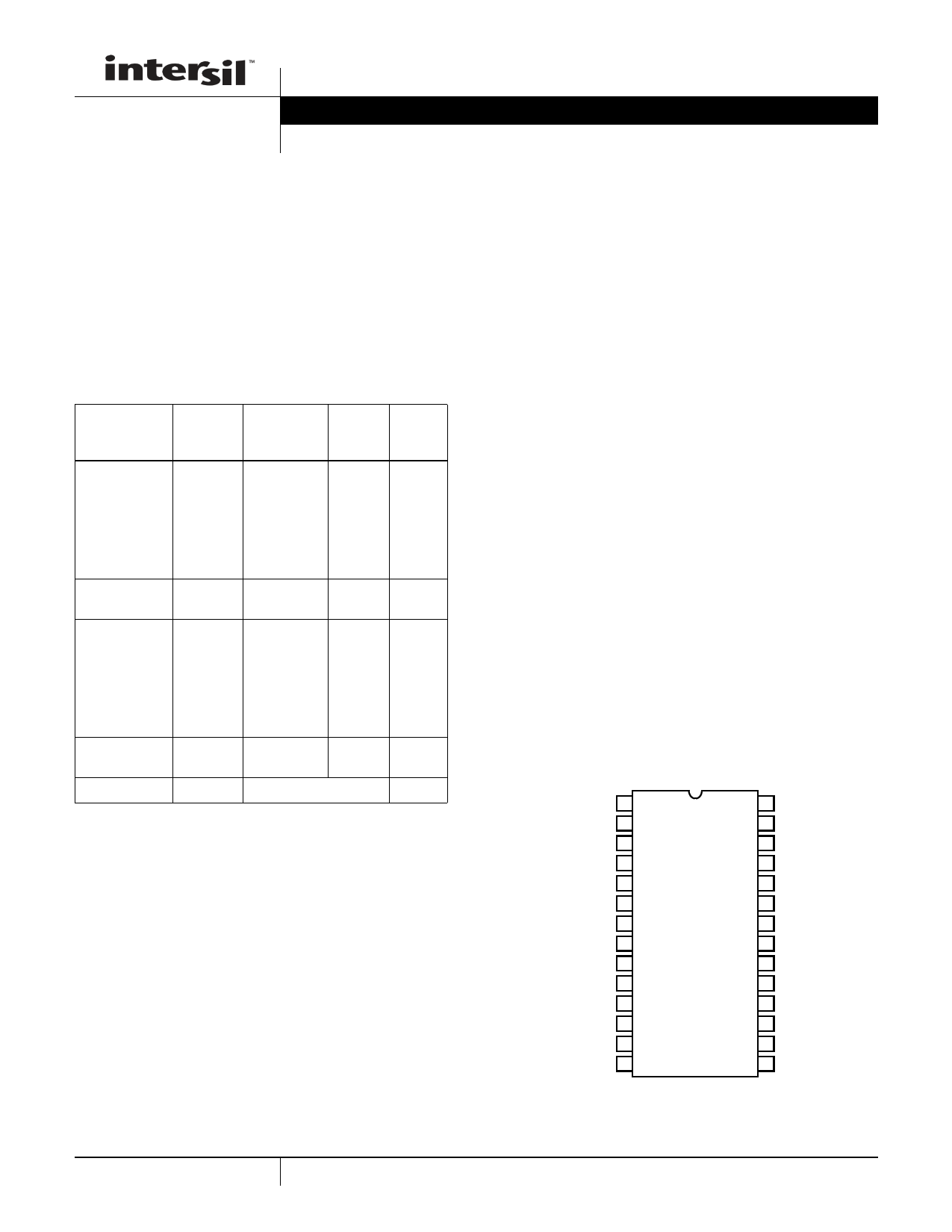
Pinout
ISL5861
TOP VIEW
D11 (MSB) 1
D10 2
D9 3
D8 4
D7 5
D6 6
D5 7
D4 8
D3 9
D2 10
D1 11
D0 (LSB) 12
DCOM 13
DCOM 14
28 CLK
27 DVDD
26 DCOM
25 NC
24 AVDD
23 COMP
22 IOUTA
21 IOUTB
20 ACOM
19 NC
18 FSADJ
17 REFIO
16 REFLO
15 SLEEP
1
CAUTION: These devices are sensitive to electrostatic discharge; follow proper IC Handling Procedures.
1-888-INTERSIL or 321-724-7143 | Intersil and Design is a trademark of Intersil Americas LLC
Copyright © Intersil Americas LLC 2001, 2004, 2015 All Rights Reserved
1 page 
ISL5861
Electrical Specifications
PARAMETER
AVDD = DVDD = +3.3V, VREF = Internal 1.2V, IOUTFS = 20mA, TA = 25oC for All Typical Values (Continued)
TA = -40oC TO 85oC
TEST CONDITIONS
MIN TYP MAX UNITS
Spurious Free Dynamic Range,
SFDR to Nyquist (fCLK/2)
fCLK = 210MSPS, fOUT = 80.8MHz (Notes 4, 7)
- 51 - dBc
fCLK = 210MSPS, fOUT = 40.4MHz (Notes 4, 7, 9)
- 60 - dBc
fCLK = 200MSPS, fOUT = 20.2MHz, T = 25oC (Notes 4, 7)
60 62 - dBc
fCLK = 200MSPS, fOUT = 20.2MHz, T = -40oC to 85oC (Notes 4, 7) 58
-
- dBc
fCLK = 130MSPS, fOUT = 50.5MHz (Notes 4, 7)
- 57 - dBc
fCLK = 130MSPS, fOUT = 40.4MHz (Notes 4, 7)
- 62 - dBc
fCLK = 130MSPS, fOUT = 20.2MHz (Notes 4, 7)
- 69 - dBc
fCLK = 130MSPS, fOUT = 10.1MHz (Notes 4, 7)
- 73 - dBc
fCLK = 130MSPS, fOUT = 5.05MHz, T = 25oC (Notes 4, 7)
70 77 - dBc
fCLK = 130MSPS, fOUT = 5.05MHz, T = -40oC to 85oC (Notes 4, 7) 68
-
- dBc
fCLK = 100MSPS, fOUT = 40.4MHz (Notes 4, 7)
- 60 - dBc
fCLK = 80MSPS, fOUT = 30.3MHz (Notes 4, 7)
- 63 - dBc
fCLK = 80MSPS, fOUT = 20.2MHz (Notes 4, 7)
- 69 - dBc
fCLK = 80MSPS, fOUT = 10.1MHz (Notes 4, 7, 9)
- 70 - dBc
fCLK = 80MSPS, fOUT = 5.05MHz (Notes 4, 7)
- 76 - dBc
fCLK = 50MSPS, fOUT = 20.2MHz (Notes 4, 7)
- 68 - dBc
fCLK = 50MSPS, fOUT = 10.1MHz (Notes 4, 7)
- 73 - dBc
fCLK = 50MSPS, fOUT = 5.05MHz (Notes 4, 7)
- 77 - dBc
Spurious Free Dynamic Range,
fCLK = 210MSPS, fOUT = 28.3MHz to 45.2MHz, 2.1MHz Spacing,
-
65
-
dBc
SFDR in a Window with Eight Tones 50MHz Span (Notes 4, 7, 9)
fCLK = 130MSPS, fOUT =17.5MHz to 27.9MHz, 1.3MHz Spacing,
-
68
-
dBc
35MHz Span (Notes 4, 7)
fCLK = 80MSPS, fOUT = 10.8MHz to 17.2MHz, 811kHz Spacing, - 75 - dBc
15MHz Span (Notes 4, 7)
fCLK = 50MSPS, fOUT = 6.7MHz to 10.8MHz, 490kHz Spacing,
10MHz Span (Notes 4, 7)
- 77 - dBc
Spurious Free Dynamic Range,
fCLK = 78MSPS, fOUT = 11MHz, in a 20MHz Window, RBW=30kHz
-
90
-
dBc
SFDR in a Window with EDGE or GSM (Notes 4, 7, 9)
Adjacent Channel Power Ratio,
ACPR with UMTS
fCLK = 76.8MSPS, fOUT = 19.2MHz, RBW=30kHz (Notes 4, 7, 9) - 70 -
dB
VOLTAGE REFERENCE
Internal Reference Voltage, VFSADJ
Internal Reference Voltage Drift
Pin 18 Voltage with Internal Reference
1.2 1.23
1.3
V
- 40 - ppm/oC
Internal Reference Output Current
Sink/Source Capability
Reference is not intended to be externally loaded
- 0 - A
Reference Input Impedance
- 1 - M
Reference Input Multiplying Bandwidth (Note 7)
- 1.0 - MHz
DIGITAL INPUTS D11-D0, CLK
Input Logic High Voltage with
3.3V Supply, VIH
Input Logic Low Voltage with
3.3V Supply, VIL
Sleep Input Current, IIH
(Note 3)
(Note 3)
2.3 3.3
-
- 0 1.0
-25 - +25
V
V
A
5
5 Page 
ISL5861
REQ = 0.5 x (RLOAD // RDIFF)
AT EACH OUTPUT
PIN 21
PIN 22
ISL5861
IOUTB
RDIFF
IOUTA
VOUT = (2 x IOUTA x REQ)V
1:1
RLOAD
RLOAD REPRESENTS THE
LOAD SEEN BY THE TRANSFORMER
FIGURE 13. OUTPUT LOADING FOR DATASHEET
MEASUREMENTS
REQ = 0.5 x (RLOAD // RDIFF// RA), WHERE RA=RB
AT EACH OUTPUT
PIN 21
PIN 22
ISL5861
IOUTB
IOUTA
RA
RDIFF
RB
VOUT = (2 x IOUTA x REQ)V
RLOAD
Propagation Delay
The converter requires two clock rising edges for data to be
represented at the output. Each rising edge of the clock
captures the present data word and outputs the previous
data. The propagation delay is therefore 1/CLK, plus <2ns of
processing. See Figure 15.
Test Service
Intersil offers customer-specific testing of converters with a
service called Testdrive. To submit a request, fill out the
Testdrive form. The form can be found by doing an ‘entire
site search’ at www.intersil.com on the words ‘DAC
Testdrive’. Or, send a request to the technical support center.
RLOAD REPRESENTS THE
LOAD SEEN BY THE TRANSFORMER
FIGURE 14. ALTERNATIVE OUTPUT LOADING
Timing Diagram
CLK
D11-D0
IOUT
tPW1
tPW2
tSU
W0
tHLD
tSU
W1
tPD
tHLD
tSU
W2
tPD
OUTPUT=W0
tHLD
50%
W3
OUTPUT=W-1
OUTPUT=W1
FIGURE 15. PROPAGATION DELAY, SETUP TIME, HOLD TIME AND MINIMUM PULSE WIDTH DIAGRAM
11
11 Page | ||
| Páginas | Total 14 Páginas | |
| PDF Descargar | [ Datasheet ISL5861.PDF ] | |
Hoja de datos destacado
| Número de pieza | Descripción | Fabricantes |
| ISL5861 | High Speed D/A Converter | Intersil |
| Número de pieza | Descripción | Fabricantes |
| SLA6805M | High Voltage 3 phase Motor Driver IC. |
Sanken |
| SDC1742 | 12- and 14-Bit Hybrid Synchro / Resolver-to-Digital Converters. |
Analog Devices |
|
DataSheet.es es una pagina web que funciona como un repositorio de manuales o hoja de datos de muchos de los productos más populares, |
| DataSheet.es | 2020 | Privacy Policy | Contacto | Buscar |