|
|
PDF LC75836WS-T Data sheet ( Hoja de datos )
| Número de pieza | LC75836WS-T | |
| Descripción | General-Purpose LCD Driver | |
| Fabricantes | ON Semiconductor | |
| Logotipo | ||
Hay una vista previa y un enlace de descarga de LC75836WS-T (archivo pdf) en la parte inferior de esta página. Total 18 Páginas | ||
|
No Preview Available !
LC75836WS-T
CMOS LSI
1/4-Duty
General-Purpose LCD Driver
Overview
The LC75836WS-T is 1/4-duty general-purpose microprocessor-
controlled LCD driver that can be used in applications such as
frequency display in products with electronic tuning. In addition to
being able to drive up to 140 segments directly, the LC75836WS-T
can also control up to 4 general-purpose output ports.
www.onsemi.com
SPQFP48 7x7 / SQFP48
Features
1/4 duty, 1/3 bias drive (Up to 140 segment can be displayed.)
Serial data input supports CCB* format communication with the system controller (support 3V operation).
Serial data control of the power-saving mode based backup function and the all segments forced off function.
Serial data control of switching between the segment output port and general-purpose output port functions.
Serial data control of the frame frequency of the common and segment output waveforms.
Either RC oscillator operating or external clock operating mode can be selected with the serial control data.
High generality, since display data is displayed directly without the intervention of a decoder circuit.
The INH pin allows the display to be forced to the off state.
RC oscillation circuit (with external resistor and capacitor)
CCB is ON Semiconductor® ’s original format. All addresses are managed
by ON Semiconductor® for this format.
CCB is a registered trademark of Semiconductor Components Industries, LLC.
ORDERING INFORMATION
See detailed ordering and shipping information on page 18 of this data sheet.
© Semiconductor Components Industries, LLC, 2015
June 2015 - Rev. 0
1
Publication Order Number :
LC75836WS-T/D
1 page 
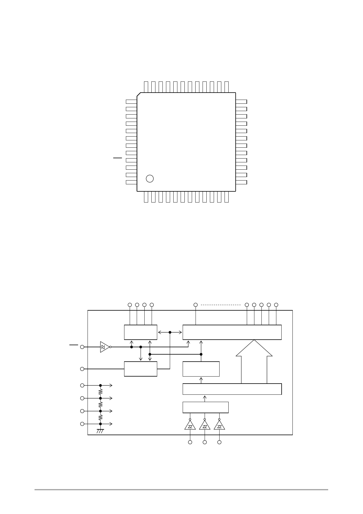
Pin Assignment
LC75836WS-T
COM3
COM4
S35
VDD
VDD1
VDD2
VSS
OSC
INH
CE
CL
DI
36 25
37 24
LC75836WS-T
48 13
1 12
S24
S23
S22
S21
S20
S19
S18
S17
S16
S15
S14
S13
Top view
Block Diagram
INH
OSC
VDD
VDD1
VDD2
VSS
COMMON
DRIVER
CLOCK
GENERATOR
SEGMENT DRIVER & LATCH
CONTROL
REGISTER
SHIFT REGISTER
CCB INTERFACE
www.onsemi.com
5
5 Page 
LC75836WS-T
5. BU: Normal mode/power-saving mode control data
This control data bit selects either normal mode or power saving mode.
BU Mode
0 Normal mode
Power saving mode.
In RC oscillator operating mode (OC = 0), the OSC pin oscillator is stopped, and in external clock operating mode
1 (OC = 1), acceptance of the external clock is stopped. In this mode the common and segment output pins go to the
VSS levels. However, S1/P1 to S4/P4 output pins that are set to be general-purpose output ports by the control data
P0 to P2 can be used as general-purpose output ports.
www.onsemi.com
11
11 Page | ||
| Páginas | Total 18 Páginas | |
| PDF Descargar | [ Datasheet LC75836WS-T.PDF ] | |
Hoja de datos destacado
| Número de pieza | Descripción | Fabricantes |
| LC75836WS-T | General-Purpose LCD Driver | ON Semiconductor |
| Número de pieza | Descripción | Fabricantes |
| SLA6805M | High Voltage 3 phase Motor Driver IC. |
Sanken |
| SDC1742 | 12- and 14-Bit Hybrid Synchro / Resolver-to-Digital Converters. |
Analog Devices |
|
DataSheet.es es una pagina web que funciona como un repositorio de manuales o hoja de datos de muchos de los productos más populares, |
| DataSheet.es | 2020 | Privacy Policy | Contacto | Buscar |
